When germanium is doped with phosphorus, the doped material has


Download our appand get started for free
Experience the future of education. Simply download our apps or reach out to us for more information. Let's shape the future of learning together!No signup needed.*
Similar Questions
- 1In $P$-type semiconductor the majority and minority charge carriers are respectivelyView Solution
- 2View SolutionWhich statement is correct
- 3View SolutionWhich one is reverse-biased
- 4The correct curve between voltage gain $\left(A_v\right)$ and load resistance $\left(R_L\right)$ isView Solution
- 5Consider the following statements $A$ and $B$ and identify the correct choice of the given answers$A$ : The width of the depletion layer in a $P-N$ junction diode increases in forwards bias$B$ : In an intrinsic semiconductor the fermi energy level is exactly in the middle of the forbidden gapView Solution
- 6In a forward biased $P N$-ju nction diode, the potential barrier in the depletion region is of the form ...View Solution
- 7When the $P$ end of $P-N$ junction is connected to the negative terminal of the battery and the $N$ end to the positive terminal of the battery, then the $P-N$ junction behaves likeView Solution
- 8In the circuit of a triode valve, there is no change in the plate current, when the plate potential is increased from $200$ volt to $220$ volt and the grid potential is decreased from $-0.5$ volt to $-1.3$ volt. The amplification factor of this valve isView Solution
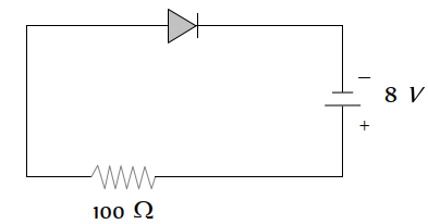
- 9A source voltage of $8 V$ drives the diode in fig. through a currentlimiting resistor of $100 ohm$. Then the magnitude of the slope load line on the $V-I$ characteristics of the diode isView Solution
- 10View SolutionIn an insulator, the forbidden energy gap between the valence band and conduction band is of the order of