Which is the correct diagram of a half-wave rectifier
- A
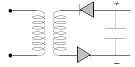
- B
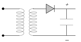
- C
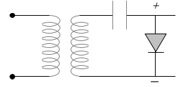
- D
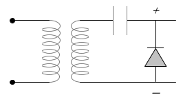
[Orissa PMT 2004]


Download our appand get started for free
Experience the future of education. Simply download our apps or reach out to us for more information. Let's shape the future of learning together!No signup needed.*
Similar Questions
- 1View SolutionIn a semiconductor the separation between conduction band and valence band is of the order of
- 2In a semiconducting material the mobilities of electrons and holes are $\mu$ and $\mu$ respectively. Which of the following is trueView Solution
- 3On increasing the reverse bias to a large value in a $P N$-junction diode, currentView Solution
- 4In a $P-N$ junction diode if $P$ region is heavily doped than $n$ region then the depletion layer isView Solution
- 5With a change of load resistance of a triode, used as an amplifier, from $50$ kilo ohms to $100$ kilo ohms, its voltage amplification changes from $25$ to $30.$ Plate resistance of the triode isView Solution
- 6View SolutionSymbolic representation of photodiode is
- 7View SolutionCorrect relation for triode is
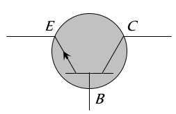
- 8View SolutionThe symbol given in figure represents
- 9View SolutionA full wave rectifier circuit along with the input and output voltages is shown in the figure Output voltage
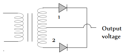
The contribution to output voltage from diode -2 is - 10Which of the following statements concerning the depletion zone of an unbiased $P N$ junction is (are) trueView Solution