Questions · Page 3 of 5

M.C.Q [1M]

MCQ 1011 Mark
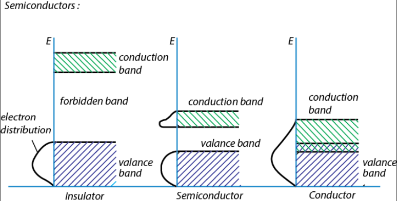
In intrinsic semiconductors:
  • A
    n > p
  • B
    p > n
  • C
    n = p
  • D
    n = 0
Answer
  1. n = p

Explanation:

Intrinsic semiconductors are pure ones. Hence there is no question of impurity. Valence band is the range of energy of electrons which are in the valence shell of the atoms of a substance. Conduction band is the range of energy of electrons which are free and available for conduction.

At room temperature, some electrons of intrinsic semiconductors get excited and reach the conduction band. During this process, the electrons leave empty spaces in the valence shell. These empty spaces are known as holes in a semiconductor. Number of free electrons (n) is equal to the number of holes (p).

View full question & answer
MCQ 1021 Mark
Statement -1: NAND and NOR gates are called digital building blocks.
Statement-2: The repeated use of NAND (or NOR) gates can produce all the basis or complicated gates.
  • A
    Statement -1 is false, Statement -2 is true.
  • B
    Statement 1-is true, Statement -2 is true and Statement -2 is correct explanation of Statement-1.
  • C
    Statement 1-is true, Statement -2 is true and statement -2 is not correct explanation of statement-1.
  • D
    Statement 1-is true, Statement -2 is false.
Answer
  1. Statement 1-is true, Statement -2 is true and Statement -2 is correct explanation of Statement-1.

Explanation:

NAND or NOR gates are called universal gates or digital building blocks. Also, the repeated use of NAND (or NOR) gates can produce all the basis or any complicated gates can be formed using NAND (or NOR) gates. Hence, statement 1-is true statement -2 is true statement -2 is correct explanation of statement-1.

View full question & answer
MCQ 1031 Mark
If the bandgap between valence band and conduction band in a material is 0eV, then the material is:
  • A
    Semiconductor
  • B
    Good conductor
  • C
    Superconductor
  • D
    Insulator
Answer
  1. Good conductor

Explanation:

In good conductors, the valance band and the conduction band overlap each other resulting in a zero band gap energy. Whereas, bandgap in insulator is nearly 5 eV and that in semiconductors is nearly 1.1eV.

Hence the given material is a good conductor.

View full question & answer
MCQ 1041 Mark
The conduction band and valency band of a good conductor are:
  • A
    Well separated.
  • B
    Just touch.
  • C
    Very close.
  • D
    Overlapped.
Answer
  1. Overlapped.

Explanation:

In conductors, electrons are loosely bound to the nucleus hence, can detach easily at room temperature also. A large number of free electrons thus, available are conduction electrons.

The energy level of these electrons corresponds to the conduction level, hence valance level and conduction level are overlapped.

View full question & answer
MCQ 1051 Mark
The concepts of holes is introduced based on:
  • A
    The notion that it is a whole lot easier to keep track of the missing particles in an "almost-full" band.
  • B
    The keeping track of the actual electrons in that band.
  • C
    The charge of holes
  • D
    None of the above
Answer
  1. The notion that it is a whole lot easier to keep track of the missing particles in an "almost-full" band.

Explanation:

The concept of holes was introduced so as to occupy the empty spaces left by the missing electron. For example, in a valence band, when an electron jumps from valence to conduction band, an empty space is created in valence band which is occupied by a hole.

View full question & answer
MCQ 1061 Mark
Forbidden gap in a pure conductor is:
  • A
    0 eV
  • B
    0.7 eV
  • C
    1.1 eV
  • D
    6 eV
Answer
  1. 0 eV

Explanation:

Forbidden band gap is the group of energy levels that cannot be occupied by the electrons, these energies lies in between conduction band and valence band. In pure conductors, electrons are loosely bound to the nucleus hence, can detach easily at room temperature also.

A large number of free electrons thus, available are conduction electrons. The energy level of these electrons corresponds to the conduction level, hence valence level and conduction level are overlapped.

Due to this, there is no forbidden band gap present in between conduction band and valence band hence, for metals the forbidden band gap is 0 eV.

View full question & answer
MCQ 1071 Mark
Which of the following statement(s) is/are true about holes?
  • A
    They flow from positive terminal to negative terminal.
  • B
    They flow from negative terminal to positive terminal.
  • C
    They do not flow
  • D
    None of these
Answer
  1. They flow from positive terminal to negative terminal.

Explanation:

Electrons flow from negative to positive terminal of battery. whenever the electric current flows from positive terminal of battery to negative terminal of battery is called conventional current. the conventional current has same direction of flow of holes but opposite to direction of flow of from electron.

View full question & answer
MCQ 1081 Mark
To reduce the ripples in a rectifier circuit with capacitor filter:
  • A
    RL should be increased.
  • B
    Input frequency should be decreased.
  • C
    Input frequency should be increased.
  • D
    Capacitors with high capacitance should be used.
Answer
  1. RL should be increased.
  1. Input frequency should be increased.
  2. ​​​​​Capacitors with high capacitance should be used.

Solution:

Ripple factor may be defined as the ratio of r.m.s. value of the ripple voltage to the absolute value of the DC component of the output voltage, usually expressed as a percentage. However ripple voltage is also commonly expressed as the peak-to-peak value. Ripple factor (r) of a full wave rectifier using capacitor filter is given by

$\text{r}=\frac{0.236\text{R}}{\omega\text{L}}$

where, L is inductance of the coil and $\omega$ is the angular frequency.

or Ripple factor can also be given by

$\text{r}=\frac{1}{4\sqrt{3}\text{v}\text{R}_\text{L}\text{C}_\text{V}}$

i.e., $\text{r}\propto\frac{1}{\text{R}_\text{L}}\Rightarrow\ \text{r}\propto\frac{1}{\text{C}},\text{r}\propto\frac{1}{\text{V}}$

Ripple factor is inversely proportional to RL, C and v.

Thus to reduce r, RL should be increased, input frequency v should be increased and capacitance C should be increased.

View full question & answer
MCQ 1091 Mark
In the Boolean algebra, the following one is wrong:
  • A
    1 + 0 = 1
  • B
    0 + 1 = 1
  • C
    1 + 1 = 1
  • D
    0 + 0 = 1
Answer
  1. 0 + 0 = 1

Explanation:

In the Boolean algebra, binary addition is given as:

1 + 0 = 1

0 + 1= 1

1 + 1 = 1

Hence, 0 + 0 =1 is wrong.

View full question & answer
MCQ 1101 Mark
The cause of the potential barrier in a p-n diode is:
  • A
    Depletion of positive charges near the junction.
  • B
    Concentration of positive charges near the junction.
  • C
    Depletion of negative charges near the junction.
  • D
    Concentration of positive and negative charges near the junction.
Answer
  1. Concentration of positive and negative charges near the junction.

Explanation:

During the formation of a junction diode, holes from p- region diffuse into n-region and electrons from n-region diffuse into p-region.

In both cases, when an electrons meets a hole, they cancel the effect at each other and as a result, a thin layer at the junction becomes free from any of charges carriers. This is called depletion layer.

There is a potential gradient in the depletion layer, negative on the p-side, and positive on the n-side.

The potential difference thus developed across the junction is called potential barrier.

View full question & answer
MCQ 1111 Mark
The breakdown in a reverse biased p-n junction diode is more likely to occur due to.
  • A
    Large velocity of the minority charge if the doping concentration is small.
  • B
    Large velocity of the minority charge carriers if the doping concentration is small.
  • C
    Strong electric field in a depletion region if the doping concentration is small.
  • D
    Strong electric filed in the deplention region if the doping conentration is large.
Answer
  1. Large velocity of the minority charge if the doping concentration is small.

Explanation:

When it comes to he breakdown in a reverse biased PN junction diode, it will probably happen only because of the accumulation of the higher charge at the biased region and large velocity of the minority charge if the doping concentration is small. This is the main cause the breakdown.

View full question & answer
MCQ 1121 Mark
The distinction between conductors, insulators and semiconductors is largely concerned with:
  • A
    Their ability to conduct current
  • B
    The type of crystal lattice
  • C
    Binding energy of their electrons
  • D
    Relative widths of their energy gaps
Answer
  1. Relative widths of their energy gaps

Explanation:

According to band theory, distinction between conductors, insulators and semiconductors is based on relative width of energy gaps between valence band and conduction band.

View full question & answer
MCQ 1131 Mark
Electric current is due to drift of electrons in:
  • A
    Metallic conductors
  • B
    Semiconductors
  • C
    Both (a) and (b) above
  • D
    None of the above
Answer
  1. Metallic conductors

Explanation:

When an electric field is applied across the metallic conductors the randomly moving electrons are subjected to electrical forces along the direction of the field. Due to this field, the electrons do not give up their randomness of motion, but they will be shifting towards higher potential. That means the electrons will drift towards higher potential along with their random motions.

In semiconductors, in addition to electrons, the travelling vacancies in the valence-band electron population (called 'holes'), act as mobile positive charges and are treated as charge carriers. Electrons and holes are the charge carriers in semiconductors.

Hence, electric current is due to drift of electrons in metallic conductors.

View full question & answer
MCQ 1141 Mark
The diffusion current in a p-n junction is:
  • A
    From the n-side to the p-side
  • B
    From the p-side to the n-side
  • C
    From the n-side to the p-side if the junction is forward-biased and in the opposite direction if it is reverse-biased
  • D
    From the p-side to the n-side if the junction is forward-biased and in the opposite direction if it is reverse-biased
Answer
  1. From the p-side to the n-side

Explanation:

Holes from p-type diffuse into the n-type and electrons from n-type diffuse into the p-type due to concentration gradient to form a depletion region which results in the rise of diffusion current flowing from p to n side.

View full question & answer
MCQ 1151 Mark
In positive logic, the logic state 1 corresponds to:
  • A
    Positive voltage
  • B
    Zero voltage
  • C
    Lower voltage level
  • D
    Higher voltage level
Answer
  1. Higher voltage level

Explanation:

In digital logic, higher voltage is defined as logic state '1' and lower voltage is defined as logic state '0'. The higher voltage need not necessarily be positive. For example, it is possible that state '0' is defined as −10 V and state '1' is defined as −5 V.

View full question & answer
MCQ 1161 Mark
Which of the following is an example of a direct band gap intrinsic semiconductor?
  • A
    Silicon
  • B
    Germanium
  • C
    Gallium Arsenide
  • D
    None of these
Answer
  1. Gallium Arsenide

Explanation:

Direct Band gap: Defined when maximum energy in the valence band and minimum energy in the conduction band occurs at the same values of the crystal momentum i.e, a direct transition of electrons from valence to conduction band takes place.

View full question & answer
MCQ 1171 Mark
LEDs have the following advantages over conventional incandescent low power lamps: 
  • A
    Long life and ruggedness.
  • B
    Low operational voltage and less power
  • C
    Fast on-off switching capability.
  • D
    All of the above
Answer
  1. All of the above

Explanation:

LEDs have longer life as compared to incandescent lamps. LED require low operational voltage and less power as compared to incandescent lamps. LEDs also have fast on-off switching capabilities.

View full question & answer
MCQ 1181 Mark
In the circuit shown in Fig., if the diode forward voltage drop is 0.3V, the voltage difference between A and B is:

  • A
    1.3V.
  • B
    2.3V.
  • C
    0.
  • D
    0.5V.
Answer
  1. 2.3V.

Solution:

If V is the potential difference between A and B, then according to the questions and using Kirchhoff’s law, we have

V - 0.3 = [(5+ 5)103] × (0.2 × 1(10-3))

⇒ V - 0.3 = [(5 + 5)103] × (0.2 × 10-3)

⇒ V - 0.3 = 10 × 103 × 0.2 × 10-3 = 2

⇒ V = 2 + 0.3 = 2.3V

View full question & answer
MCQ 1191 Mark
In semiconductors, at room temperature:
  • A
    The conduction band is completely empty.
  • B
    The valence band is partially empty and the conduction band is partially filled.
  • C
    The valence band is completely filled and the conduction band is partially filled.
  • D
    The valence band is completely filled.
Answer
  1. The valence band is completely filled and the conduction band is partially filled.
View full question & answer
MCQ 1201 Mark
LCD stands for:
  • A
    Light Carrying Diode
  • B
    Liquid Crystal Display
  • C
    Long Crystal Display
  • D
    Light Crystal Display
Answer
  1. Liquid Crystal Display

    Explanation:

    LCD stands for "Liquid Crystal Display".

LCD is a special thin flat panel that can let light go through it, or can block the light. (Unlike an LED it does not produce its own light).

The panel is made up of several blocks, and each block can be in any shape. Each block is filled with liquid crystals that can be made clear or solid, by changing the electric current to that block.

View full question & answer
MCQ 1211 Mark
What happens during regulation action of a Zener diode?
  • A
    The current in and voltage across the Zenor remains fixed.
  • B
    The current through the series Resistance (Rs) changes.
  • C
    The Zener resistance is constant.
  • D
    The resistance offered by the Zener changes.
Answer
  1. The current through the series Resistance (Rs) changes.
  1. The resistance offered by the Zener changes.

Solution:

Symbolically zener diode represents like this:

In the forward bias, the zener diode acts as an ordinary diode. It can be used as a voltage regulator.

A zener diode when reverse biases offers constant voltage drop across in terminals as unregulated voltage is applied across circuit to regulate. Then during regulation action of a Zener diode, the current through the series resistance Rs changes and resistance offered by the Zener changes. The current through the Zener changes but the voltage across the Zener remains constant.

View full question & answer
MCQ 1221 Mark
For detecting the light_______________.
  • A
    The photodiode has to be forward biased.
  • B
    The photodiode has to be reversed biased.
  • C
    The LED has to connected in forward bias mode.
  • D
    The LED has to be connected in reverse bias mode.
Answer
  1. The photodiode has to be reversed biased.

Explanation:

Photo diode is used to detect light.

In reverse biased condition, the width of depletion region increases as the the applied reverse bias voltage increases across the diode. So, by applying a larger voltage, more of the incident photons are converted to electric current thereby increasing the efficiency.

In forward biased condition, the width of depletion region decreases so only a small portion of the incident photons get converted to electric current and hence the efficiency is less.

Hence photo diode in reverse biased condition detects light.

View full question & answer
MCQ 1231 Mark
A 220 V A.C. supply is connected between points A and B (Fig.). What will be the potential difference V across the capacitor?

  • A
    220V.
  • B
    110V.
  • C
    0V.
  • D
    $220\sqrt{2}\text{V}.$
Answer
  1. $220\sqrt{2}\text{V}.$

Solution:

Key concept: Half wave rectifier: When the P-N junction diode rectifies half of the ac wave, it is called half wave rectifier.

  1. During positive half cycle,

Diode → Forward biased

Output signal → obtained

  1. During negative half cycle,

Diode → reverse biased

Output signal → not obtained

  1. Output voltage is obtained across the load resistance RL. It is not constant but pulsating (mixture of ac and dc) in nature.
  2. Average output in one cycle

$\text{I}_\text{dc}=\frac{\text{I}_0}{\pi}\text{ and }\text{V}_\text{dc}=\frac{\text{V}_0}{\pi};\text{I}_0=\frac{\text{V}_0}{\text{r}_\text{f}+\text{R}_\text{I}}$

(rf = forward biased resistance)

  1. r.m.s. output: $\text{I}_\text{rms}=\frac{\text{I}_0}{2},\text{V}_\text{rms}=\frac{\text{V}_0}{2}$

As p-n junction diode will consuct during positive half cycle only, during negative half cycle diode is reverse biased. During this diode will not give any output. So, potential difference across capacitor C = peak voltage of the given AC voltage

$=\text{V}_0=\text{V}_\text{rms}\sqrt{2}=220\sqrt{2}\text{V}$

View full question & answer
MCQ 1241 Mark
Zener diode works on:
  • A
    Zero bias
  • B
    Reverse bias
  • C
    Forward bias
  • D
    Infinite bias
Answer
  1. Reverse bias

Explanation:

We know that zener diode works on the reverse bias. When the reverse bias is equal to the break-down voltage, the voltage across the zener remains almost constant and the current increases rapidly.

View full question & answer
MCQ 1251 Mark
Which logic gate produces LOW output when any of the inputs is HIGH?
  • A
    AND
  • B
    OR
  • C
    NAND
  • D
    NOR
Answer
  1. NOR

Explanation:

The truth table for NOR gate is shown above which suggests that NOR gate is the logic gate which produces low output when any of the inputs is high.

View full question & answer
MCQ 1261 Mark
p-n junction diode acts as:
  • A
    ohmic resistance
  • B
    non-ohmic resistance
  • C
    both A and B
  • D
    amplifier
Answer
  1. non-ohmic resistance

Explanation:

We know that in the case of metallic conductors, the potential difference varies in direct proportion to the current flowing. The I−V graph of a ohmic conductor is a straight line. But, a p-n junction diode is not in according with Ohm's law. The current voltage characteristic curve of a p-n junction diode shows both forward bias as well as reverse bias characteristics as shown as in the graph.

View full question & answer
MCQ 1271 Mark
Zener diode is used for:
  • A
    Amplification
  • B
    Rectification
  • C
    Stabilisation
  • D
    All of the above
Answer
  1. Stabilisation

Explanation:

A zener diode is always operated in its reverse biased condition. A voltage regulator circuit can be designed using a zener diode to maintain a constant DC output voltage across the load in spite of variations in the input voltage or changes in the load current. The zener voltage regulator consists of a current limiting resistor RS​ connected in series with the input voltage VS​ with the zener diode connected in parallel with the load RL in this reverse biased condition.Hence we can say that ,zener diode is used for stabilization.

View full question & answer
MCQ 1281 Mark
The electrical conductivity of pure germanium can be increased by:
  • A
    Increasing the temperature.
  • B
    Doping acceptor impurities.
  • C
    Doping donor impurities.
  • D
    All of the above.
Answer
  1. All of the above.
View full question & answer
MCQ 1291 Mark
In physics, chemistry, and electronic engineering, _______________ is the lack of an electron at a position where one could exist in an atom or atomic lattice.
  • A
    An electron hole
  • B
    Electron
  • C
    Proton
  • D
    Neutron
Answer
  1. An electron hole

Explanation:

A hole is an absence of an electron in a particular place in an atom. Although it is not a physical particle, a hole can be passed from atom to atom in a semiconductor material.

View full question & answer
MCQ 1301 Mark
Which of these is the best description of a Zener diode?
  • A
    It is a constant voltage device.
  • B
    It operates in the reverse region.
  • C
    It is a constant current device.
  • D
    It works in forward region.
Answer
  1. It is a constant voltage device.

Explanation:

Zener diode is a p-n junction diode working in the breakdown region. It is used as a voltage regulator/stabilizer to provide a constant voltage from a source whose voltage may fluctuate over a wide range.

View full question & answer
MCQ 1311 Mark
The zone in a semiconductor diode where no free charge carriers exists is known as the:
  • A
    Anode region
  • B
    Cathode region
  • C
    Depletion region
  • D
    None of these
Answer
  1. Depletion region

Explanation:

In depletion region negative charge carrier electrons are attached with their positive charge carrier holes. hence there is no free charge carriers exists.

View full question & answer
MCQ 1321 Mark
In reverse biasing:
  • A
    Large amount of current flows.
  • B
    Potential barrier across junction increases.
  • C
    Depletion layer resistance increases.
  • D
    No current flows.
Answer
  1. Potential barrier across junction increases.
View full question & answer
MCQ 1331 Mark
In an LED device, the intensity of emitted light:
  • A
    Increases continuously with the forward current of the diode.
  • B
    Increases continuously with the forward current of the diode, reaches a maximum and then decreases.
  • C
    Decreases continuously with the forward current of the diode.
  • D
    Decreases continuously with the forward current of the diode, reaches a minimum and then increases.
Answer
  1. Increases continuously with the forward current of the diode, reaches a maximum and then decreases.

Explanation:

The intensity of emitted light increase with the foreword current more the light intensity.

View full question & answer
MCQ 1341 Mark
NAND and NOR gates are called universal gates primarily because they:
  • A
    Are available universally.
  • B
    Can be combined to produce OR, AND and NOT gates.
  • C
    Are widely used in Integrated circuit packages.
  • D
    Are easiest to manufacture.
Answer
  1. Can be combined to produce OR, AND and NOT gates.
View full question & answer
MCQ 1351 Mark
The vacancy created due to the absence of an electron in the valence band of a semiconductor is called a _________ .
  • A
    Electron
  • B
    Hole
  • C
    Proton
  • D
    Position
Answer
  1. Hole

Explanation:

Whenever an electron jumps from a valence band to conduction band, an equal and opposite charge is left behind in the place of an electron. This is called a hole.

View full question & answer
MCQ 1361 Mark
In insulators________. (C.B is conduction band and V.B is valence band)
  • A
    V.B. is partially filled with electrons.
  • B
    C.B. is partially filled with electrons.
  • C
    C.B. is empty and V.B. is filled with electrons.
  • D
    C.B. is filled with electrons and V.B. is empty.
Answer
  1. C.B. is empty and V.B. is filled with electrons.

Explanation:

As shown in the image, insulators have a very large forbidden gap. Their conduction band is empty, thus they cannot conduct electricity under normal room temperature and pressure conditions. The valence band is full.

View full question & answer
MCQ 1381 Mark
In a photo-diode, 
  • A
    Photocurrent is proportional to incident light intensity.
  • B
    Photocurrent is inversely proportional to incident light intensity.
  • C
    Photocurrent is independent of the incident light intensity.
  • D
    Incident light intensity is proportional to the photocurrent.
Answer
  1. Photocurrent is proportional to incident light intensity.

Explanation:

In a photodiode, photocurrent is directly proportional to intensiy of incident light. More the incident light intensity, more will be the current produced.

View full question & answer
MCQ 1391 Mark
Let nh and ne be the number of holes and conduction electrons in an extrinsic semiconductor:
  • A
    nh > ne.
  • B
    nh = ne.
  • C
    nh < ne.
  • D
    nh ≠ ne.
Answer
  1. nh ≠ ne.
View full question & answer
MCQ 1401 Mark
The breakdown in a reverse biased p-n junction diode is more likely to occur due to:
  • A
    Large velocity of the minority charge carriers if the doping concentration is small.
  • B
    Large velocity of the minority charge carriers if the doping concentration is large.
  • C
    Strong electric field in a depletion region if the doping concentration is small.
  • D
    Strong electric field in the depletion region if the doping concentration is large.
Answer
  1. Large velocity of the minority charge carriers if the doping concentration is small.
  1. Strong electric field in the depletion region if the doping concentration is large.

Solution:

Reverse biasing: Positive terminal of the battery is connected to the N-crystal and negative terminal of the battery is connected to P-crystal.

  1. In reverse biasing width of depletion layer increases
  2. In reverse biasing resistance offered RReverse = 105Ω.
  3. Reverse bias supports the potential barrier and no current flows across the junction due to the diffusion of the majority carriers.

(A very small reverse current may exist in the circuit due to the drifting of minority carriers across the junction)

  1. Break down voltage: Reverse voltage at which break down of semiconductor occurs. For Ge it is 25V and for Si it is 35V.

So, we conclude that in reverse biasing, ionization takes place because the minority charge carriers will be accelerated due to reverse biasing and striking with atoms which in turn cause secondary electrons and thus more number of charge carriers.

When doping concentration is large, there will be a large number of ions in the depletion region, which will give rise to a strong electric field.

View full question & answer
MCQ 1411 Mark
In an insulator, the energy gap between conduction band and valence band is about:
  • A
    0 eV
  • B
    6 eV
  • C
    1 eV
  • D
    0.6 eV
Answer
  1. 6 eV

Explanation:

Atoms are neutral in the insulator, thus there are no valence electrons in the outer orbit. The electrons are tightly bound with the nucleus hence, at room temperature thermal energy is not enough to push the electrons into conduction band and hence, no electrons are available for conduction.

The energy required for electron to escape out from orbit and to over come the energy gap is thus of the order of 6 eV.

View full question & answer
MCQ 1421 Mark
For one electron vacancy,
  • A
    no holes are created
  • B
    1 hole is created
  • C
    2 holes are created
  • D
    4 holes are created
Answer
  1. 1 hole is created

Explanation:

For one electron vacancy, an empty space or void is created. In order to fill that empty space, a charge carrier with a charge equal in magnitude but opposite polarity should occupy that space in order to maintain electrical neutrality. Such a charge particle is called a hole.

View full question & answer
MCQ 1431 Mark
In a metal, the separation between conduction band and valence band is of the order:
  • A
    100 eV
  • B
    10 eV
  • C
    0 eV
  • D
    1 eV
Answer
  1. 0 eV

Explanation:

Energy band gap is the energy difference between conduction band and valence band, i. e., energy required to an electron to overcome the energy levels between conduction band and valence band. In conductors, electrons are loosely bound to the nucleus hence, can detach easily at room temperature also.

A large number of free electrons thus, available are conduction electrons. The energy level of these electrons corresponds to the conduction level, hence valance level and conduction level are overlapped. Due to this, there is no gap between conduction band and valence band hence, for metals their separation is of the order of 0 eV.

View full question & answer
MCQ 1441 Mark
To get an output Y=1 from the circuit above, the input must be:
  • A
    A-0 B-1 C-0
  • B
    A-1 B-0 C-0
  • C
    A-1 B-0 C-1
  • D
    A-1 B-1 C-0
Answer
  1. A-1 B-0 C-1

Explanation:

Logic gate OR is used for addition of the input signals and Logic gate AND is used for multiplication of the input signals. Hence, here inputs A = 1, B = 0 and C = 1 will yield the output Y = 1.

View full question & answer
MCQ 1451 Mark
In the Boolean algebra, the following one is wrong:
  • A
    1.0 = 0
  • B
    0.1 = 0
  • C
    1.1 = 0
  • D
    1.1 = 1
Answer
  1. 1.1 = 0

Explanation:

In the Boolean algebra,

1.0 = 0

0.1 = 0

1.1 = 1

View full question & answer
MCQ 1461 Mark
When a hole is produced in P-type semiconductor, there is:
  • A
    Extra electron in valence band
  • B
    Extra electron in conduction band
  • C
    Missing electron in valence band
  • D
    Missing electron in conduction band
Answer
  1. Missing electron in valence band

Explanation:

A hole is not itself a physical quantity but a missing electron in valence band. An electron from adjacent site jumps to fill this hole and thus creates a hole at its former site. So it seems as if the hole itself has moved.

View full question & answer
MCQ 1471 Mark
In Boolean algebra, Y = A + B implies that:
  • A
    Output Y exists when both inputs A and B exist.
  • B
    Output Y exists when either input A exists or input B exists or both inputs A and B exist.
  • C
    Output Y exists when either input A exists or input B exists but not when both inputs A and B exist.
  • D
    Output Y exists when both inputs A and B exists but not when either input A or B exist.
Answer
  1. Output Y exists when both inputs A and B exist.
View full question & answer
MCQ 1481 Mark
A semiconductor is a material with a small but non-zero band gap that behaves as an insulator at absolute zero but allows thermal excitation of electrons into its ____________ at temperatures that are below its melting point.
  • A
    HOMO
  • B
    Valence band
  • C
    Conduction band
  • D
    LUMO
Answer
  1. Conduction band

Explanation:

The band gap in case of semiconductors is of order 3−4 eV. At absolute zero, the valence band is filled and conduction band is empty, so it behaves as an insulator. As the temperature is raised, electrons in the valence band gain sufficient energy to overcome the band gap and jump to the conduction band.

View full question & answer
MCQ 1491 Mark
A pure semiconductor at absolute zero has:
  • A
    Absence of electrons in the conduction band.
  • B
    All the electrons occupying the valence band.
  • C
    Large Eg​ value.
  • D
    All of the above.
Answer
  1. All of the above.

Explanation:

At absolute zero temperature, in a pure semiconductor, all electrons occupy the valence band and no electrons are present in the conduction band. The forbidden gap energy Eg​ is large.

View full question & answer
MCQ 1501 Mark
The gate that has only one input terminal:
  • A
    NOT
  • B
    NOR
  • C
    NAN
  • D
    XOR
Answer
  1. NOT

Explanation:

Only one logic gate has one input terminal i.e. NOT gate.

View full question & answer