Questions · Page 2 of 2

3 Marks Question

Question 513 Marks
Draw the circuit diagram of a full wave rectifier and explain its working. Also, give the input and output waveforms.
Answer

Full-wave rectifier:
Two diodes are used to give rectified O/ P corresponding to both positive as well as negative half cycles.

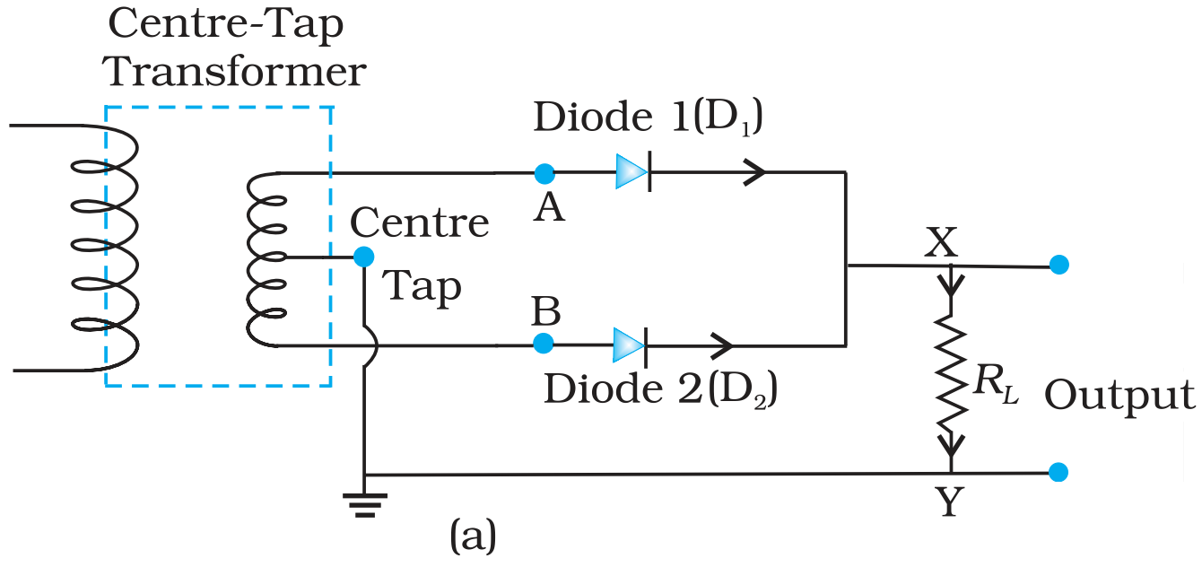
When the voltage at $A$ with respect to the center tap is positive, and the voltage at $B$ is negative. Then, $D_1$ is forward biased and $D_2$ is reversed biased. Hence, $D_1$ conducts and $D_2$ does not.
When the voltage of $A$ becomes negative, then $B$ becomes + ve. Therefore, $D_1$ does not conduct and $D_2$ conducts. Hence, we obtain output voltage during both the positive as well as negative half of the cycle.
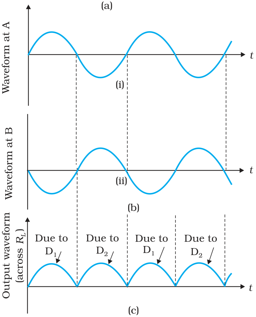
Input and Output waveforms are shown below.
View full question & answer
Question 523 Marks
  1. Three photo diodes $D_1, D_2$ and $D_3$ are made of semiconductors having band gaps of 2.5eV, 2eV and 3eV respectively. Which of them will not be able to detect light of wavelength 600nm?
  2. Why photodiodes are required to operate in reverse bias? Explain.
Answer
  1. Energy of the incident light
$\text{E}=\frac{\text{hC}}{\lambda}$

$=\frac{(6.6\times10^{-34})\times(3\times10^8)}{(600\times10^{-9})\times(1.6\times10^{-19})}$

$\text{E}=2.06\text{eV}$

The incident radiations can be detected by a photodiode if the energy of incident radiation photon is greater than the band gap. This is true only for $D_2(2eV)$. Hence, only $D_2$ will detect the light of 600nm wavelength.
  1. The photodiode is reverse biased for operating in the photoconductive mode. As the photodiode is in reverse bias, the width of the depletion layer increases. This reduces the junction capacitance and thereby the response time. In effect, the reverse bias causes faster response times for the photodiode. The photocurrent is linearly proportional to the illuminance.
View full question & answer
Question 533 Marks
A p-n junction germanium diode when forward biased has a drop of 0.3V which is assumed to be independent of current. The current in excess of 10mA through the diode produces a large Joule-heating which damages (burns) the diode. If we want to use a 1.5V battery to forward-bias the diode, what should be the value of resistor used in series with the diode, so that the maximum current does not exceed 6mA?
Answer
The basic equation of diode-circuit is:
$\text{RI}+\text{V}_0=\text{V}_\text{B}$
$\Rightarrow\text{R}=\frac{\text{V}_\text{E}-\text{V}_0}{\text{I}}$
Here, $\text{V}-\text{B}=1.5\text{V},\text{V}_0$
$=0.3\text{V},\text{I}=5\text{mA}=6\times10^{-3}\text{A}$
$\therefore\text{R}=\frac{1.5-0.3}{6\times10^{-3}}$
$=\frac{1.2\times10^{3}}{6}$
$=0.2\times10^3\Omega$
$=200\Omega$
View full question & answer
Question 543 Marks
The following table gives the output of a two input logic gate.
  1. Identify the logic gate and draw its logic symbol.
  2. If the output of this gate is fed as input to a NOT gate, name the new logic gate so formed.
A
B
Y
0
0
1
1
0
1
0
1
1
1
1
0
Answer

The truth table given represents a NAND gate.

Clearly resulting gate will be an AND gate.

Truth table of new gate formed,
Input Output
A B Y $\bar{\text{Y}}=\text{Z}$
0 0 1 0
0 1 1 0
1 0 1 0
1 1 0 0
View full question & answer
Question 553 Marks
For the transistor circuit shown in Fig, evaluate $V_E, R_B, R_E$ given $I_C = 1\ mA, V_{CE} = 3V, V_{BE} = 0.5\ V$ and $V_{CC} = 12\ V, \beta = 100.$
Answer
As, $I_C ≈ I_E$
$\therefore IC (RC + RE) + VCE = 12V$
$RE = 9 - RC = 1.2KΩ$
$\therefore VE = 1.2V$
$V_B = V_E + V_{BE} = 1.7V$
$\text{I}=\frac{\text{V}_\text{B}}{20\text{K}}=0.085\text{mA}$
$\text{R}_\text{B}=\frac{12-1.7}{\frac{\text{I}_\text{c}}{\beta}+0+085}=\frac{10.3}{0.01+0.085}=108\text{k}\Omega$
View full question & answer
Question 563 Marks
There are energy bands in a solid. Do we have really continuous energy variation in a band or do we have very closely spaced but still discrete energy levels?
Answer
A solid consists of a combination of closely spaced energy levels. These energy levels are discrete but they have very small energy gap between two consecutive levels so they are referred as band. However, the energy levels in the band are discrete.
View full question & answer
Question 573 Marks
Indium antimonide has a band gap of 0.23eV between the valence and the conduction band. Find the temperature at which kT equals the band gap.
Answer
$\text{E} = 0.23\text{eV, K} = 1.38 \times 10^{-23}$
$\text{KT}=\text{E}$
$\Rightarrow 1.38 \times 10^{-23} \times \text{T} = 0.23 \times 1.6 \times 10^{-19}$
$\Rightarrow\text{T}=\frac{0.23\times1.6\times10^{-19}}{1.38\times10^{-23}}=\frac{0.23\times1.6\times10^4}{1.38}$
$=0.2676\times10^4=2670$
View full question & answer
Question 583 Marks
The band gap for silicon is 1.1eV.
  1. Find the ratio of the band gap to kT for silicon at room temperature 300K.
  2. At what temperature does this ratio become one tenth of the value at 300K?
(Silicon will not retain its structure at these high temperatures.)
Answer
Bandgap $=1.1\text{eV},\text{T}=300\text{K}$
  1. Ratio $=\frac{1.1}{\text{KT}}=\frac{1.1}{8.62\times10^{-5}\times3\times10^2}=42.53=43$
  2. $4.253'=\frac{1.1}{8.62\times10^{-5}\times\text{T}}$ or $\text{T}=\frac{1.1\times10^5}{4.253\times8.62}=3000.47\text{K}.$
View full question & answer
Question 593 Marks
In a p-n junction, the depletion region is 400nm wide and an electric field of $5 \times 10^5V/m$ exists in it.
  1. Find the height of the potential barrier.
  2. What should be the minimum kinetic energy of a conduction electron which can diffuse from the n-side to the p-side?
Answer
Let,
Depletion region width, $\text{d}=400\text{nm}=4\times10^{-7}\text{m}$
Electric field, $\text{E}=5\times10^5\text{Vm}$
Let the potential barrier be V.
The relation between the potential and the electric field is given by V = Ed
$\Rightarrow\text{V}=\text{E}\times\text{d}=5\times\text{d}$
$\Rightarrow\text{V}=5\times10^5\times4\times10^{-7}=0.2\text{V}$
To find: Kinetic energy required
Energy of any electron accelerated through a potential of V = eV
Also, the minimum energy of the electron should be equal to the band gap of the material.
$\therefore$ Potential barrier × e = 0.2eV (e = Charge of the electron).
View full question & answer
Question 603 Marks
The potential barrier existing across an unbiased p-n. junction is 0·2 volt. What minimum kinetic energy a hole should have to diffuse from the p-side to the n-side if,
  1. The junction is unbiased.
  2. The junction is forwardbiased at 0.1 volt.
  3. The junction is reverse-biased at 0.1 volt?
Answer
Potential barrier = 0.2 Volt
  1. K.E. = (Potential difference) ×e = 0.2eV (in unbiased cond$^n$)
  2. In forward biasing
KE + Ve = 0.2e
⇒ KE = 0.2e - 0.1e = 0.1e.
  1. In reverse biasing
KE - Ve = 0.2e
⇒ KE = 0.2e + 0.1e = 0.3e.
View full question & answer
Question 613 Marks
The output of an OR gate is connected to both the inputs of a NAND gate. Draw the logic circuit of this combination of gates and write its truth table.
Answer
The logic circuit is shown in fig. 
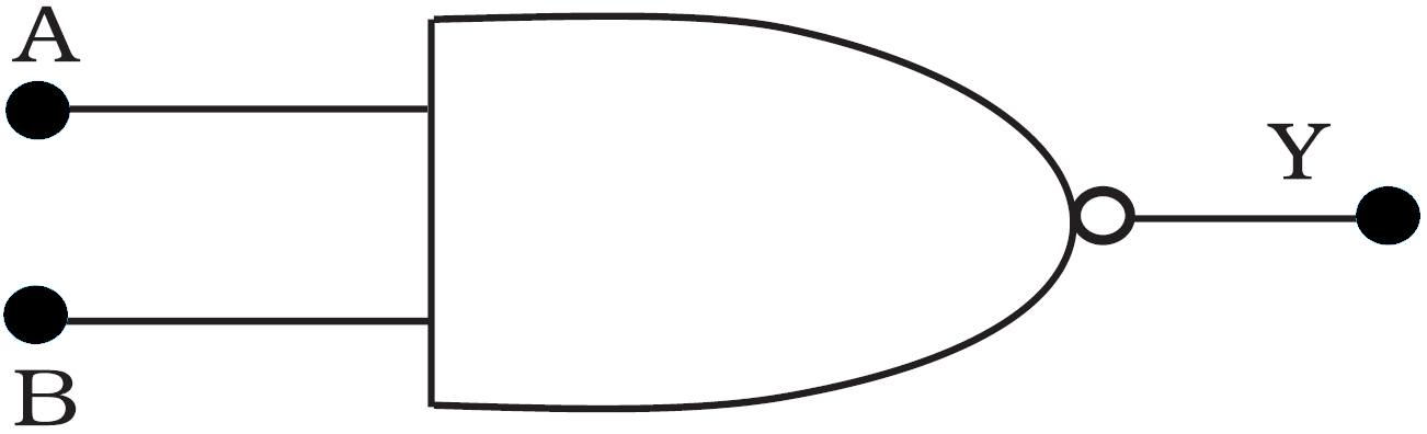
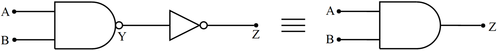
The logic circuit represents NOR gate.Its truth table is:
A
B
Y'
Y
0
0
0
1
1
0
1
0
0
1
1
0
1
1
1
0
View full question & answer
Question 623 Marks
In a p-n junction, a potential barrier of 250meV exists across the junction. A hole with a kinetic energy of 300meV approaches the junction. Find the kinetic energy of the hole when it crosses the junction if the hole approached the junction.
  1. From the p-side.
  2. From the n-side.
Answer
Potential barrier ‘d’ = 250meV
Initial KE of hole = 300meV
We know: KE of the hole decreases when the junction is forward biased and increases when reverse blased in the given ‘Pn’ diode.
So,
  1. Final KE = (300 - 250)meV = 50meV.
  2. Initial KE = (300 + 250)meV = 550meV.
View full question & answer
Question 633 Marks
In a common emitter mode of a transistor, the d.c. current gain is 20, the emitter current is 7mA. Calculate (i) base current and (ii) collector current.
Answer
Given, $\beta=20,\text{i}_\text{E}=7\text{mA}$
  1. $\beta=\frac{\text{i}_\text{C}}{\text{i}_\text{B}}=\frac{\text{e}_\text{E}-\text{i}_\text{B}}{\text{i}_\text{B}}$ or $\beta_{\text{i}_\beta}=\text{i}_\text{E}=\text{i}_\text{B}$
$\Rightarrow\text{i}_\text{B}=\frac{\text{i}_\text{E}}{\beta+1}$

$=\frac{7\text{mA}}{20+1}=\frac{7}{21}\text{mA} $

$=\frac13\text{mA}$
  1. $\text{i}_\text{C}=\text{i}_\text{E}-\text{i}_\text{B}=7-\frac13=\frac{20}{3}\text{mA}$
View full question & answer
Question 643 Marks
In a silicon transistor, the base current is changed by $20\mu\text{A}.$ This results in a change of 0.02V in base to emitter voltage and a change of 2mA in the collector current.
  1. Find the input resistance, $\beta-$ac and trans conductance of the transistor.
  2. This transistor is used as an amplifier in CE configuration with a load resistance $5\text{k}\Omega$ What is the voltage gain of the amplifier?
Answer
Given $\Delta\text{I}_\text{B} = 20\mu\text{A} = 20 \times 10^{-3}\text{mA} = 0.020\text{mA,}$
$\Delta\text{V}_\text{BE} = 0.02\text{V}, \Delta\text{I}_\text{C} = 2\text{mA}$
Input resistance, $\text{R}_\text{i}=\frac{\Delta\text{V}_\text{BE}}{\Delta\text{I}_\text{B}}=\frac{ 0.02}{20\times10^{-6}}\Omega=10^3\Omega=1\text{k}\Omega$
Current gain, $\beta_\text{ac}=\frac{\Delta\text{I}_\text{C}}{\Delta\text{I}_\text{B}}=\frac{\text{2mA}}{0.020\text{mA}}=100$
Trans conductance of a transistor is defined as the ratio of change in collector current to the change in base to emitter voltage at constant collector to emitter voltage, i.e.,
$\text{gm}=\Big(\frac{\Delta\text{I}_\text{C}}{\Delta\text{V}_\text{BE}}\Big)_{\text{V}_\text{CE} =\text{cons}\tan}\text{t}=\frac{2\times10^{-3}}{0.02}=0.1\text{W}^{-1}$
Voltage gain, $\text{A}_\text{v}=\frac{\text{R}_\text{L}}{\text{R}_\text{i}}\times\beta$
Given $\text{RL}=5\text{k}\Omega=5\times103\Omega,$
$\therefore\text{A}_\text{v}=\frac{5\times10^3}{1000}\times1000=500$
As CE amplifier causes a phase shift of 180° between input and output voltages, so voltage gain, $A_ν = -500$.
View full question & answer
Question 653 Marks
Estimate the proportion of boron impurity whieh will increase the conductivity of a pure silicon sample by a factor of 100. Assume that each boron atom creates a hole and the concentration of holes in pure silicon at the same temperature is $7 \times 10^{15}$ holes per cubic metre. Density of silicon is $5 \times 10^{21}$ atoms per cubic metre.
Answer
Total no.of charge carriers initially $=2\times7\times10^{15}=14\times10^{15}$ Cubic meter.
Finally the total no.of charge carriers $=14\times10^{17}\text{m}^3$
We know,
The product of the concentrations of holes and conduction electrons remains, almost the same.
Let x be the no.of holes.
So, $\big(7\times10^{15}\big)\times\big(7\times10^{15}\big)=\text{x}\times\big(14\times10^{17}-\text{x}\big)$
$\Rightarrow14\text{x}\times10^{17}-\text{x}^2=79\times10^{30}$
$\Rightarrow\text{x}^2-14\text{x}\times10^{17}-49\times10^{30}=0$
$\text{x}=\frac{14\times10^{17}\pm14^2\times\sqrt{10^{34}+4\times49\times10^{30}}}{2}$ $=14.00035\times10^{17}.$
= Increased in no. of holes or the no.of atoms of Boron added.
⇒ 1 atom of Boron is added per $\frac{5\times10^{28}}{1386.035\times10^{15}}$ $=3.607\times10^{-3}\times10^{13}=3.607\times10^{10}.$
View full question & answer
Question 663 Marks
We have valence electrons and conduction electrons in a semiconductor. Do we also have 'valence holes' and 'conduction holes'?
Answer
Holes do not exist in reality. They exist only virtually. When an electron jumps from the valence band to the conduction band, a vacancy is created at the place from where the electron had jumped. This vacancy is called a hole. So, a valence or conduction hole is a virtual concept only.
View full question & answer
Question 673 Marks
Explain the following:
  1. In the active state of the transistor, the emitter base junction acts as a low resistance while base collection region acts as high resistance.
  2. Output characteristics are controlled by the input characteristics in common emitter transistor amplifier.
  3. EDs are made of compound semiconductor and not by elemental semiconductors.
Answer
  1. Emitter base junction is forward biased whereas collector base junction is reverse biased.
  2. Small change in the current IB in the base circuit controls the large current IC in the collector circuit $\text{I}_\text{C}=\beta\text{I}_\text{B}.$
  3. Elemental semiconductor’s band gap is such that the emitted wavelength lies in IR region. Hence cannot be used for making LED.
View full question & answer
Question 683 Marks
If each diode in Fig. has a forward bias resistance of 25Ω and infinite resistance in reverse bias, what will be the values of the current $I_1, I_2, I_3$ and $I_4?$
Answer
$I_3$ is zero as the diode in that branch is reverse, so,
Resistance in branch $AB = 25 + 125 = 150Ω,$ (let $R_1$)
Resistance in branch $EF = 25 + 125 = 150Ω.$ (let $R_2$)
As AB and EF are identical parallel branches, their effective resistance is $150/2 = 75Ω.$
Net resistance in the circuit $= (75 + 25) = 100W .$
Now, Current $I_1 = 5/100 = 0.05A$
As resistances of AB and EF are equal, and $I_1 = I_2 + I_3 + I_4, I_3 = 0$
So, $I_2 = I_4 = 0.025A.$
View full question & answer
Question 693 Marks
In a pure semiconductor, the number of conduction electrons is $6 \times 10^{19}$ per cubic metre. How many holes are there in a sample of size 1cm × 1cm × 1mm?
Answer
In a pure semiconductor, the no. of conduction electrons = no. of holes
Given volume $=1\text{cm}\times1\text{cm}\times1\text{mm}$
$=1\times10^{-2}\times1\times10^{-2}\times1\times10^{-3}=10^{-7}\text{m}^3$
No.of electrons $=6\times10^{19}\times10^{-7}=6\times10^{12}$
Hence no.of holes $=6\times10^{12}$
View full question & answer
Question 703 Marks
The conductivity of a pure semiconductor is roughly proportional to $\text{T}^\frac{3}{2}\text{e}^{\frac{-\Delta\text{E}}{2\text{kT}}}$ where $\Delta\text{E}$ is the band gap. The band gap for germanium is 0.74eV at 4K and 0.67eV at 300K. By what factor does the conductivity of pure germanium increase as the temperature is raised from 4K to 300K?
Answer
$\sigma=\text{T}^\frac{3}{2}\text{e}^\frac{-\Delta\text{E}}{2\text{KT}}\text{ at }4^\circ\text{K}$
$\sigma=4^\frac{3}{2}=\text{e}^{\frac{-0.67}{{2\times8.62\times10^{-5}\times4}}}=8\times\text{e}^{-1073.08}$
$\text{At } 300\text{K},$
$\sigma=300^\frac{3}{2}\text{ e}^{\frac{-0.67}{{2\times8.62\times10^{-5}\times300}}}=\frac{3\times1730}{8}\text{e}^{-12.95}$
$\text{Ratio}=\frac{8\times\text{e}^{-1073.08}}{\Big[\frac{3\times1730}{8}\Big]\times\text{e}^{-12.95}}=\frac{64}{3\times1730}\text{e}^{-1060.13}$
View full question & answer
Question 713 Marks
Answer the following question:
  1. Write the truth table of the following gate.
  1. What will be the values of inputs A and B for the Boolean expression.
$\text{A}\bar{+}\text{B}).(\text{A}\bar{.}\text{B})=1$
Answer
Truth table of the given gate:
Input   Output
A B Y = A + AB
0 0 0
1 0 1
0 1 0
1 1 1
A = 0, B = 0
Other then $(\text{A}\bar{+}\text{B}).(\overline{\text{AB}})=(0\bar{+}0)(0\bar{.}0)=\bar{0}.\bar{0}=1.1=1$
View full question & answer
Question 723 Marks
The band gap between the valence and the conduction bands in zinc oxide (ZnO) is 3.2eV. Suppose an electron in the conduction band combines with a hole in the valence band and the excess energy is released in the form of electromagnetic radiation. Find the maximum wavelength that can be emitted in this process.
Answer
Given:
Band gap = 3.2eV
As the electron in the conduction band combines with the hole in the valence band, the minimum energy band gap (because maximum energy is released) through which the electron has to jump will be equal to the band gap of the material.
This implies that the maximum energy released in this process will be equal to the band gap of the material.
Here,
$\text{E}=3.2\text{eV}$
Thus,
$\Rightarrow3.2\text{eV}=\frac{1242\text{eV}-\text{nm}}{\lambda}$
$\Rightarrow\lambda=388.1\text{nm}$
View full question & answer
Question 733 Marks
The product of the hole concentration and the conduction electron concentration turns out to be independent of the amount of any impurity doped. The concentration of conduction electrons in germanium is $6 \times 10^{19}$ per cubic metre. When some phosphorus impurity is doped into a germanium sample, the concentration of conduction electrons increases to $2 \times 10^{23}$ per cubic metre. Find the concentration of the holes in the doped germanium.
Answer
(No. of holes) (No.of conduction electrons) = constant.
At first:
No. of conduction electrons $= 6 \times 10^{19}$
No. of holes $= 6 \times 10^{19}$
After doping
No. of conduction electrons $= 2 \times 10^{23}$
No. of holes $= x.$
$\big(6\times10^{19}\big)\big(6\times10^{19}\big)=(2\times10^{23}\big)\text{x}$
$\Rightarrow\frac{6\times6\times10^{19+19}}{2\times10^{23}}=\text{x}$
$\Rightarrow\text{x}=18\times10^{15}=1.8\times10^{16}.$
View full question & answer
Question 743 Marks
Sn, C, and Si, Ge are all group XIV elements. Yet, Sn is a conductor, C is an insulator while Si and Ge are semiconductors. Why?
Answer
The conduction level of any element depends on the energy gap between its conduction band and valence band.
In conductors, there is no energy gap between conduction band and valence band. For insulator, the energy gap is large and for semiconductor the energy gap is moderate.
The energy gap for Sn is 0eV, for C is 5.4eV, for Si is 1.1eV and for Ge is 0.7eV related to their atomic size. Therefore Sn is a conductoc, C is an insulator, and Ge and Si are semiconductors.
View full question & answer
Question 753 Marks

A Zener of power rating 1W is to be used as a voltage regulator. If zener has a breakdown of 5V and it has to regulate voltage which fluctuated between 3V and 7V, what should be the value of Rs for safe operation (Fig.)?
Answer
According to the problem, power $= 1W$
Zener breakdown voltage, $V_z = 5V$
Minimum voltage, $V_{min} = 3V$ Maximum voltage,
$V_{max} = 7V$
So current $\text{I}_{\text{Z}_\text{max}}=\frac{\text{P}}{\text{V}_\text{Z}}=\frac{1}{5}=0.2\text{A}$
For safe operation Rs will be equal to
$\text{R}_\text{s}=\frac{\text{V}_\text{max}-\text{V}_\text{z}}{\text{I}_{\text{Z}_\text{mzx}}}=\frac{7-5}{0.2}=\frac{2}{0.2}=10\Omega$
View full question & answer
Question 763 Marks
Identify the logic gate represented by the following circuit by writing its truth table:
Answer
The output of OR gate, C = A + B
The output of NAND gate, $\text{D}=\overline{\text{AB}}$
The input of AND gate are C and D, so it's output is $\text{Y}=\text{C}.\text{D}=(\text{A}+\text{B})\overline{\text{AB}}$
When $\text{A}=0,\text{ B}=0,$
$\text{ Y}=(0+0)(0\bar{\cdot}0)=(\text{}0\cdot\bar0)=0\cdot1=0$
When $\text{A}=1,\text{ B}=0,$
$\text{ Y}=(1+0)(1\bar\cdot0)=1\cdot\bar0=1\cdot1=1$
When $\text{A}=0,\text{ B}=1,$
$\text{ Y}=(0+1)(0\bar\cdot1)=1\cdot\bar0=1\cdot1=1$
When $\text{A}=1,\text{ B}=1,$
$\text{ Y}=(1+1)(1\bar\cdot1)=(1\cdot\bar1)=1\cdot0=0$
Thus, truth table of given circuit is:
A
B
Y
0
0
0
1
0
1
0
1
1
1
1
0
Thia ia the truth table of XOR gate, hence the given circuit represents XOR gate.
View full question & answer
Question 773 Marks
A semiconducting material has a band gap of 1eV. Acceptor impurities are doped into it which create acceptor levels 1meV above the valence band. Assume that the transition from one energy level to the other is almost forbidden if kT is less than $\frac{1}{50}$ of the energy gap. Also, if kT is more than twice the gap, the upper levels have maximum population. The temperature of the semiconductor is increased from 0K. The concentration of the holes increases with temperature and after a certain temperature it becomes approximately constant. As the temperature is further increased, the hole concentration again starts increasing at a certain temperature. Find the order of the temperature range in which the hole concentration remains approximately constant.
Answer
Given band gap = 1eV
Net band gap after doping $=\big(1-10^{-3}\big)\text{eV}=0.999\text{eV}$
According to the question, $\text{KT}_1=\frac{0.999}{50}$
$\Rightarrow\text{T}_1=231.78=231.8$
For the maximum limit $\text{KT}_2=2\times0.999$
$\Rightarrow\text{T}_2=\frac{2\times1\times10^{-3}}{8.62\times10^{-5}}=\frac{2}{8.62}\times10^2=23.2.$
Temperature range is (23.2 - 231.8).
View full question & answer
Question 783 Marks
A semiconductor has equal electron and hole concentration of $2 \times 10^8/m^3$. On doping with a certain impurity, the hole concentration increases to $4 × 10^{10}/m^3.$
  1. What type of semiconductor is obtained on doping?
  2. Calculate the new electron and hole concentration of the semiconductor.
  3. How does the energy gap vary with doping?
Answer
Given $n_e = 2 \times 10^8/m^3, n_h = 4 \times 10^{10}/m^3$
  1. The majority charge carriers in doped semiconductor are holes, so semiconductor obtained is p-type semiconductor.
$\text{n}_\text{e}\text{n}_h=\text{n}^2_\text{i}$
$\Rightarrow\text{n}_\text{h}=\frac{\text{n}^2_\text{i}}{\text{n}_\text{h}}$
$=\frac{(2\times10^8)^2}{4\times10^{10}}=10^6/\text{m}^3$
  1. New electron concentration $= 10^6/m^3$
Hole concentration $= 4 \times 10^{10}/m^3$
  1. Energy gap decreases on doping.
View full question & answer
Question 793 Marks
Calculate the number of states per cubic metre of sodium in 3s band. The density of sodium is $1013kg/ m^3$. How many of them are empty?
Answer
$\text{f}=1013\text{kg/ m}^3,\text{V}=1\text{m}^3$
$\text{m}=\text{fV}=1013\times1=1013\text{kg}$
No.of atoms $=\frac{1013\times10^3\times6\times10^{23}}{23}=264.26\times10^{26}$
  1. Total no.of states $=2\text{N}=2\times264.26\times10^{26}$
$=528.52=5.3\times10^{28}\times10^{26}$
  1. Total no. of unoccupied states $=2.65\times10^{26}.$
View full question & answer
Question 803 Marks
A change of 0.2mA in the base current causes a change of 5mA in the collector current for a common emitter amplifier.
  1. Find the ac current gain of the transistor.
  2. If the input resistance is $2\text{k}\Omega$ and its voltage gain is 75, calculate the load resistor used in the circuit.
Answer
  1. Ac current gain, $\beta=\frac{\Delta\text{I}_\text{C}}{\Delta\text{I}_\text{E}}=\frac{5\text{mA}}{0.2\text{mA}}=25$
  2. Voltage gain, $\text{A}_\text{V}=\beta\frac{\text{R}_\text{L}}{\text{R}_\text{i}}$
Load resistance $\text{R}_\text{L}=\frac{\text{A}_\text{v}\text{R}_\text{i}}{\beta}$
$=\frac{75\times2\times10^3}{25}$
$=60\times10^3\Omega=6\text{k}\Omega$
View full question & answer
Question 813 Marks
Give reasons for the following:
  1. The Zener diode is fabricated by heavily doping both the p and n sides of the junction.
  2. A photodiode, when used as a detector of optical signals is operated under reverse bias.
  3. The band gap of the semiconductor used for fabrication of visible LED’s must at least be 1.8eV.
Answer
  1. Heavy doping makes the depletion region very thin. This makes the electric field of the junction very high, even for a small reverse bias voltage. This in turn helps the Zener diode to act as a ‘voltage regulator’.
  2. When operated under reverse bias, the photodiode can detect changes in current with changes in light intensity more easily.
  3. The photon energy, of visible light photons varies about 1.8eV to 3eV. Hence, for visible LED’s, the semiconductor must have a band gap of 1.8eV.
View full question & answer
Question 823 Marks
Let AE denote the energy gap between the valence band and the conduction band. The population of conduction electrons (and of the holes) is roughly proportional to $\text{e}^{\frac{-\Delta\text{E}}{2\text{kT}}}.$ Find the ratio of the concentration of condu.ction electrons in diamond to that in silicon at room temperature 300K. $\Delta\text{E}$ for silicon is 1.1eV and for diamond is 6.0eV. How many conduction electrons are likely to be in one cubic metre of diamond?
Answer
Given, $\text{n}=\text{e}^{\frac{-\Delta\text{E}}{2\text{KT}}},\Delta\text{E}=\text{Diamon}\rightarrow6\text{eV};\Delta\text{E}\ \text{Si}\rightarrow1.1\text{eV}$ Now, $\text{n}_1=\text{e}^{\frac{-\Delta\text{E}_1}{2\text{KT}}}=\text{e}^{\frac{-6}{{2\times300\times8.62\times10^{-5}}}}$$\text{n}_2=\text{e}^{\frac{-\Delta\text{E}_2}{2\text{KT}}}=\text{e}^{\frac{-1.1}{{2\times300\times8.62\times10^{-5}}}}$
$\frac{\text{n}_1}{\text{n}_2}=\frac{4.14772\times10^{-51}}{5.7978\times10^{-10}}=7.15\times10^{-42}$ Due to more $\Delta\text{E},$ the conduction electrons per cubic metre in diamond is almost zero.
View full question & answer
Question 833 Marks
In a photodiode, the conductivity increases when the material is exposed to light. It is found that the conductivity changes only if the wavelength is less than 620nm. What is the band gap?
Answer
Conductivity of any material increases when the number of free charge carriers in the material increases. When a photo diode is exposed to light, additional electron hole pairs are created in the diode; thus, its conductivity increases. So to change the conductivity of a photo diode, the minimum energy of the incident radiation should be equal to the band gap of the material.
In other words,
Band gap = Energy of the incident radiation
$\Rightarrow\text{E}=\frac{\text{hc}}{\lambda}$
$\Rightarrow\text{E}=\frac{1242\text{eV}-\text{nm}}{620\text{nm}}=2.0\text{eV}$
View full question & answer
3 Marks Question - Page 2 - Physics STD 12 Science Questions - Vidyadip