Question 13 Marks
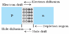
Write the two processes that take place in the formation of a p-n junction. Explain with the help of a diagram, the formation of depletion region and barrier potential in a p-n junction.
Answer
Due to the diffusion of electrons and holes across the junction a region of (immobile) positive charge is created on the n-side and a region of (immobile) negative charge is created on the p-side, near the junction; this is called depletion region.
Barrier potential is formed due to loss of electrons from n-region and gain of electrons by p-region. Its polarity is such that it opposes the movement of charge carriers across the junction.
View full question & answer→Question 23 Marks
Answer
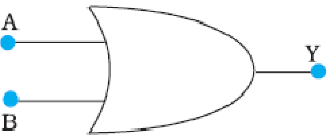
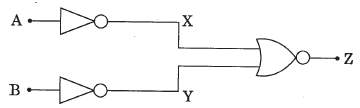
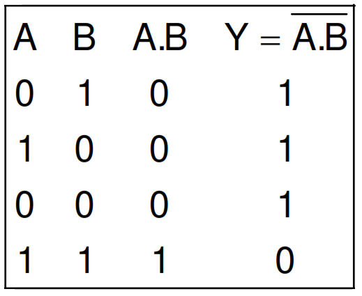
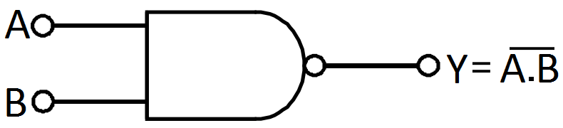
- A and Bare the inputs and Y is the output of the given circuit. The left half of the given figure acts as the NOR Gate, while the right ha1f acts as the NOT Gate. This is shown in the following figure.
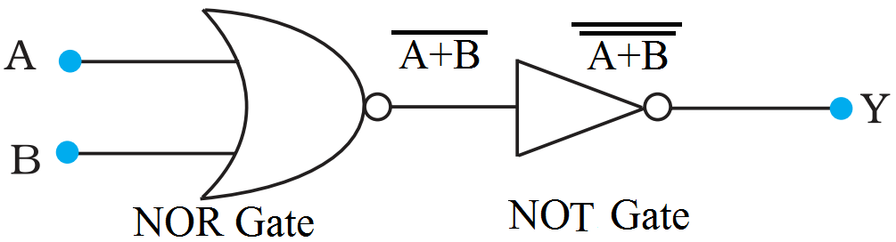
Hence, the output of the NOR Gate $=\overline{\text{A+B}}$
This will be the input for the NOT Gate. Its output wHI be ${\overline{\overline{A+B}}}=\text{A+B}$
$\therefore$ Y = A +B
Hence, this circuit functions as an OR Gate.
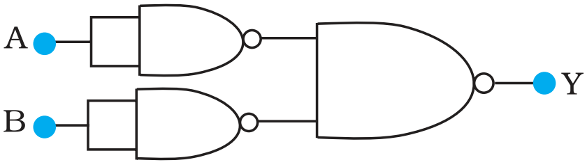
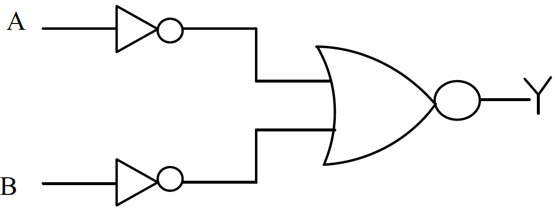
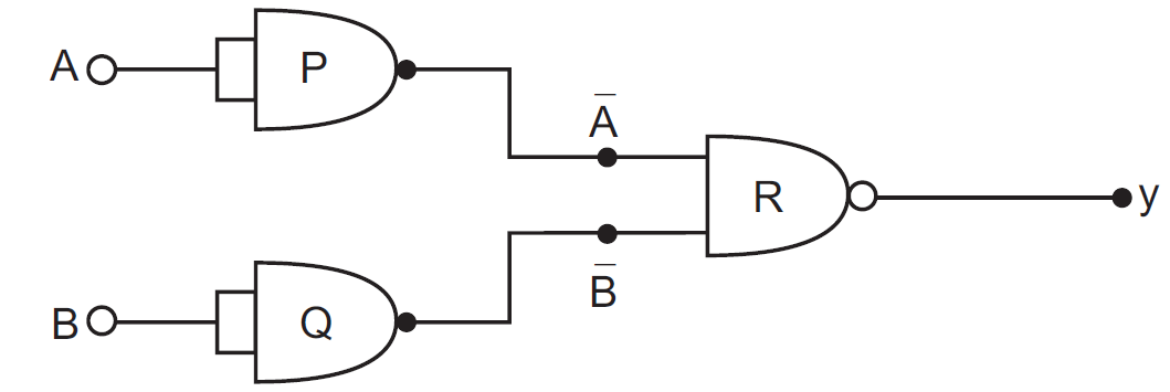
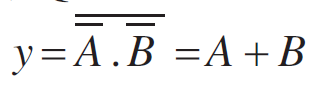
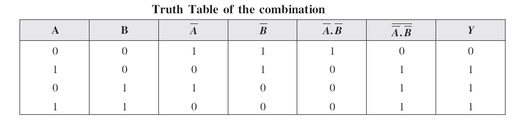
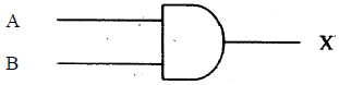
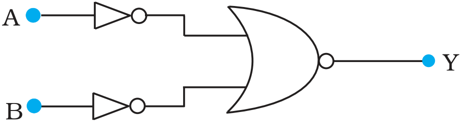
- A and B are the inputs and Y is the output of the given circuit. It can be observed from the following figure that the Inputs of the right half NOR Gate are the outputs of the two NOT Gates.
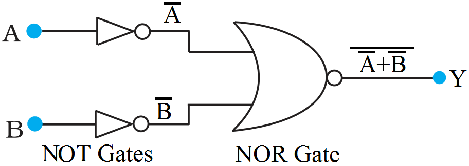
Hence, the output of the given circuit can be written as:
$ \text{Y}={\overline{\overline{\text{A}}+{\overline{\text{B}}}}}={\overline{\overline{\text{A}}\cdot{\overline{\text{B}}}}}=\text{A}\cdot\text{B}$
Hence, this circuit functions as an AND Gate. View full question & answer→Question 33 Marks
Write the truth table for circuit given in Fig. 14.47 below consisting of NOR gates and identify the logic operation (OR, AND, NOT) which this circuit is performing.
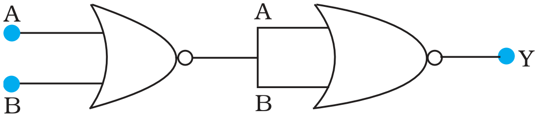
(Hint: A = 0, B = 1 then A and B inputs of second NOR gate will be 0 and hence Y=1. Similarly work out the values of Y for other combinations of A and B. Compare with the truth table of OR, AND, NOT gates and find the correct one.)
AnswerA and B are the inputs of the given circuit. The output of the first NOR gate is $\overline{\text{A}+\text{B}}.$ It can be observed from the following figure that the inputs of the second NOR gate become the out put of the first one.
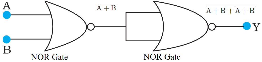
Hence, the output of the combination is given as:
$\text{Y}=\overline{\overline{\text{A}+\text{B}}+\overline{\text{A}+\text{B}}}\ =\ \bigg(\overline{\overline{\text{A}+\text{B}}}\bigg)\cdot\bigg(\overline{\overline{\text{A}+\text{B}}}\bigg)$
$=(\text{A}+\text{B})\cdot(\text{A}+\text{B})=\text{A}+\text{B}$
The truth table for this operation is given as:
|
A
|
B
|
Y (=A+B)
|
|
0
|
0
|
0
|
|
0
|
1
|
1
|
|
1
|
0
|
1
|
|
1
|
1
|
1
|
This is the truth table of an OR gate. Hence, this circuit functions as an OR gate. View full question & answer→Question 43 Marks
The number of silicon atoms per $m^3$ is $5 \times 10^{28}$. This is doped simultaneously with $5 \times 10^{22}$ atoms per $m^3$ of Arsenci and $5 \times 10^{20}$ per $m^3$ atoms of Indium. Calculate the number of electrons and holes Given that $n_i = 1.5 \times 10^{16} m^{-3}$. Is the material $n-$ type or $p-$ type?
AnswerNumber of silicon atoms $, N = 5 \times 10^{28} \text{ atoms/m^3} $ Number of arsenci atoms $, n_{As} = 5 \times 10^{22} \text{ atoms/m^3}$ Number of indium atoms $, n_{In} = 5 \times 10^{20} \text{ per m^3}$ atoms Number of thermally-generated electrons $, n_i = 1.5 \times 10^{16} \ \text{ electrons m^3}$ Number of electrons,$ n_e = 5 \times 10^{22 }-1.5 \times 10^{16 }$
$\thickapprox 4.99 \times 10^{22}$ Number of holes $= n_h$ In thermal equilibrium, the concentrations of electrons and holes in a semiconductor are related as: $n_en_h=n_i^2$
$\therefore\ \text{n}_{\text{h}}=\frac{\text{n}_\text{i}^\text{2}}{\text{n}_\text{e}}$
$=\frac{\big(1.5\times10^{16}\big)^{2}}{4.99\times10^{22}}\thickapprox4.51\times10^{9}$
Therefore, the number of electrons is approximately $4.99 \times 10^{22}$ and the number of holes is about $4.51 \times 10^9.$
Since the number of electrons is more than the number of holes, the material is an $n-$ type semiconductor.
View full question & answer→Question 53 Marks
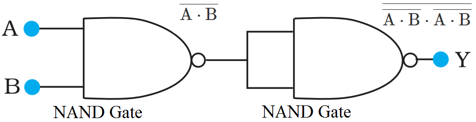
Write the truth table for a NAND gate connected as given in Fig. 14.45.
Hence identify the exact logic operation carried out by this circuit.
AnswerA acts as the two inputs of the NANO gate and Y is the output, as shown in the following figure.
Hence, the output can be written as:
$\text{Y}=\overline{\text{A}\cdot{\text{A}}}=\overline{\text{A}}+\overline{\text{A}}=\overline{\text{A}}\ \ \ ...\text{(i)}$
The truth table for equation (i) can be drawn as:
| A |
$_{\text{Y}}\Big(=\overline{\text{A}}\Big)$ |
| 0 |
1 |
| 1 |
0 |
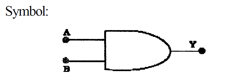
This circuit functions as a NOT gate. The symbol for this logic circuit is shown as:
View full question & answer→Question 63 Marks
A $p-n$ photodiode is fabricated from a semiconductor with band gap of $2.8\ eV$. Can it detect a wavelength of $6000\ nm$?
AnswerEnergy band gap of the given photodiode$, E_g = 2.8\ eV$
wavelength, $\lambda = 6000\ nm = 6000 \times 10^{-9} m$
The energy of a signal is given by the relation:
$\text{E}=\frac{\text{hc}}{\lambda}$
Where,
$h =$ Planck's constant
$= 6.626 \times 10^{-34} Js$
$C =$ Speed of light
$=3 \times 10^8\ m/s$
$\text{E}=\frac{6.626\times10^{-34}\times3\times10^{8}}{6000\times10^{-9}}$
$= 3.313 \times 10^{-20} J$
But $1.6 \times 10^{-19 }J = 1\ eV$
$\therefore E = 3.313 \times 10^{-20 }J$
$=\frac{3.313\times10^{-20}}{1.6\times10^{-19}}=0.207\ \text{eV}$
The energy of a signal of wavelength $6000\ nm$ is $0.207\ eV,$ which is less than $2.8\ eV -$ the energy band gap of a photodiode.
Hence, the photodiode cannot detect the signal.
View full question & answer→Question 73 Marks
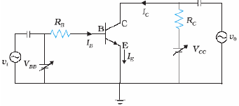
For a $CE-$transistor amplifier, the audio signal voltage across the collected resistance of $2k \Omega$ is $2 V$. Suppose the current amplification factor of the transistor is $100,$ find the input signal voltage and base current, if the base resistance is $1k \Omega$ .
AnswerCollector resistance$, R_c= 2k Ω = 2000Ω$
Audio signal voltage across the collector resistance$, V = 2 V$
Current amplification factor of the transistor$, \beta = 100$
Base resistance$, R_{B }= 1k Ω = 1000Ω$
Input signal voltage $= V_i$
Base current $= I_B$
We have the amplification relation as:
Voltage amplification $=\frac{\text{V}}{\text{V}_1}=\beta\frac{\text{R}_c}{\text{R}_B}$
$ {\text{V}_\text{i}}=\frac{\text{VR}_\text{B}}{\beta\text{R}_\text{C}}$
$=\frac{2\times1000}{100\times2000}=0.01\ \text{V}$
Therefore, the input signal voltage of the amplifier is $0.01 V$. Base resistance is given by the relation:
${\text{R}_\text{B}}=\frac{\text{V}_\text{i}}{\text{I}_\text{B}}$
$\text{I}_\text{B}=\frac{\text{V}_\text{i}}{{\text{R}_\text{B}}}$
$\text{I}_\text{B}= \frac{0.01}{1000}=10\times10\mu^{-6}\text{A}$
Therefore, the base current of the amplifier is $10 \mu\text{A}.$
View full question & answer→Question 83 Marks
You are given two circuits as shown in Fig. 14.46, which consist of NAND gates. Identify the logic operation carried out by the two circuits.
-
-
AnswerIn both the given circuits, A and B are the inputs and Y is the output.
- The output of the left NANO gate will be $\overline{{\text{A}}.\text{B}}$, as shown in the following figure.
Hence, the output of the combination of the two NAND gates is given as:
$\text{Y}=\overline{\Big(\overline{\text{A}\cdot{\text{B}}}\Big)\cdot\Big(\overline{\text{A}\cdot{\text{B}}}\Big)}=\overline{\overline{\text{AB}}}+\overline{\overline{\text{AB}}}=\text{AB}$
Hence, this circuit functions as an AND gate.
- $\overline{\text{A}}$ is the output of the upper left of the NAN D gate and $\overline{\text{B}}$ is the output of the lower half of the NAND gate, as shown in the following figure.
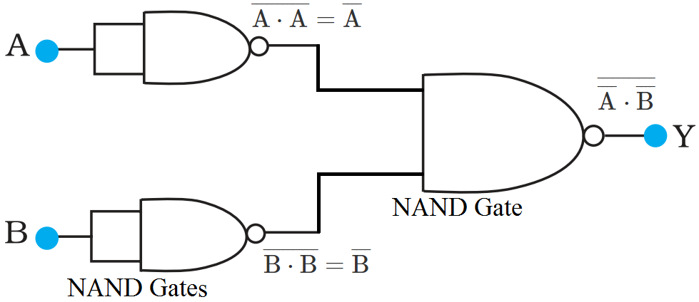
Hence, the output of the combination of the NANO gates will be given as:
$\text{Y}=\overline{\text{A}}\cdot\overline{\text{B}}=\overline{\overline{\text{A}}}+\overline{\overline{\text{B}}}=\text{A+B}$
Hence, this circuit functions as an OR gate. View full question & answer→Question 93 Marks
You are given two circuits (a) and (b) as shown in the figures, which consist of NAND gates. Identify the logic operation carried out by the two. Write the truth tables for each. Identify the gates equivalent to the two circuits.
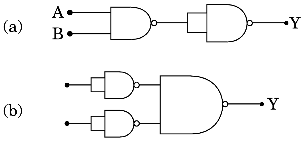
AnswerLogic Operation a) Y = A.B
b) Y = A+B
Truth Table
-
| A |
B |
Y |
| 0 |
0 |
0 |
| 1 |
0 |
0 |
| 0 |
1 |
0 |
| 1 |
1 |
1 |
-
| A |
B |
Y |
| 0 |
0 |
0 |
| 1 |
0 |
1 |
| 0 |
1 |
1 |
| 1 |
1 |
1 |
Identification:
- AND gate.
- OR gate.
View full question & answer→Question 103 Marks
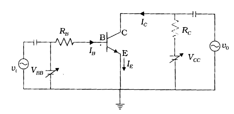
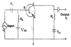
- Draw the circuit diagram of an n-p-n transistor amplifier in common emitter configuration.
- Derive an expression for voltage gain of the amplifier and hence show that the output voltage is in opposite phase with the input voltage.
Answer
-
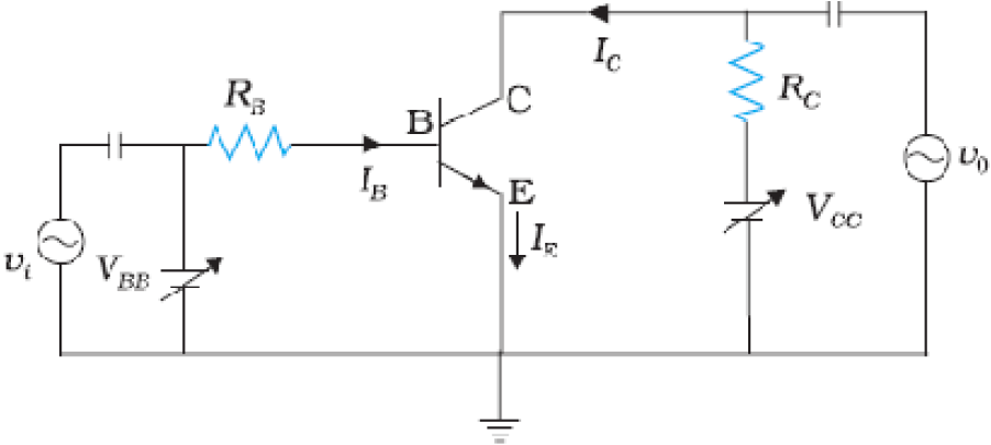
- Change in the input voltage: $\Delta {V}_{BE}=I_B{r}_i$
Change in the output voltage:$\Delta {V}_{CE}=I_C{R}_c$
Voltage gain= Output voltage/Input voltage $A_V=-\frac{\beta{{R}c}}{r_i}$
Negative sign indicates, phase difference is $180^\circ$ View full question & answer→Question 113 Marks
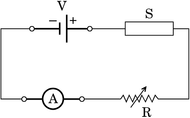
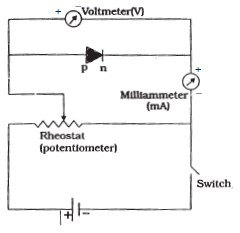
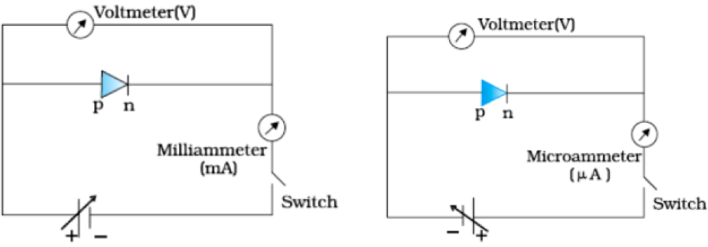
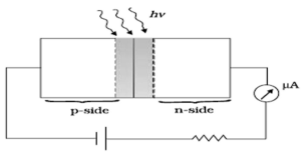
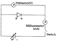
- In the following diagram ‘S’ is a semiconductor. Would you increase or decrease the value of R to keep the reading of the ammeter A constant when S is heated? Give reason for your answer.
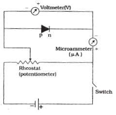
- Draw the circuit diagram of a photodiode and explain its working. Draw its I - V characteristics.
Answer
- R would be increased.
Resistance of S (a semi conductor) decreases on heating.
- Photodiode diagram:
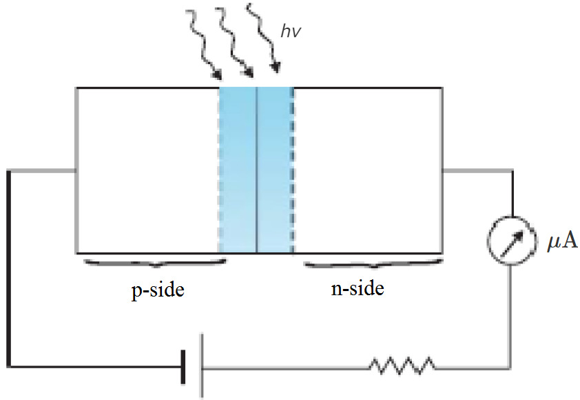
When the photodiode is illuminated with light (photons) (with energy (
hv) greater than the energy gap (Eg) of the semiconductor), then electron-hole pairs are generated due to the absorption of photons. Due to junction field, electrons and holes are separated before they recombine. Electrons are collected on n-side and holes are collected on p-side giving rise to an emf. When an external load is connected, current flows.
V-I Characteristics of the diode:
View full question & answer→Question 123 Marks
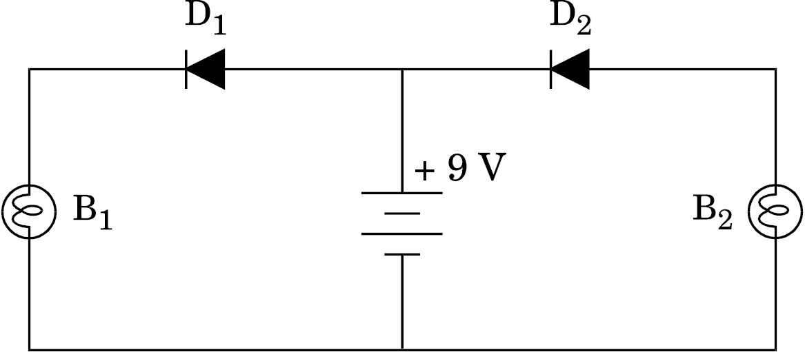
- In the following diagram, which bulb out of $B_1$ and $B_2$ will glow and why?
- Draw a diagram of an illuminated $p-n$ junction solar cell.
- Explain briefly the three processes due to which generation of emf takes place in a solar cell.
Answer
- Bulb $B_1$ glows Diode.
$D_1$ is forward biased.
- Diagram:
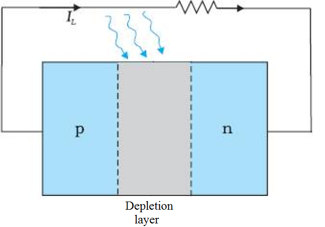
- Generation: Incident light generates electron$-$hole pairs.
Separation: Electric field of the depletion layer separates the electrons and holes.
Collection: Electrons and holes are collected at the $n$ and $p$ side contacts. View full question & answer→Question 133 Marks
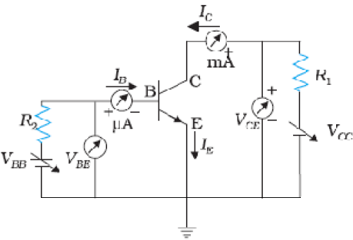
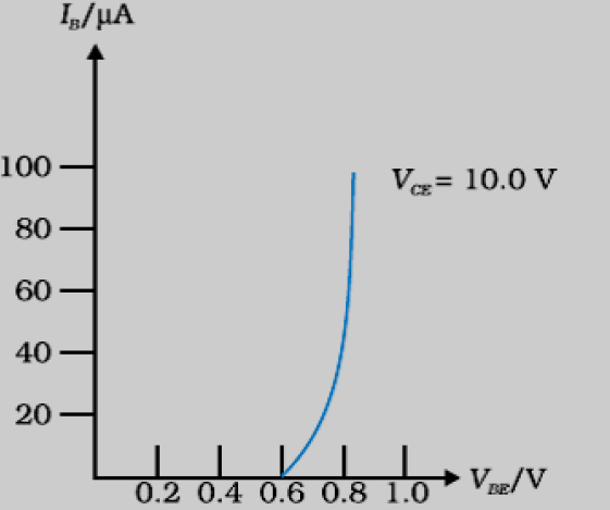
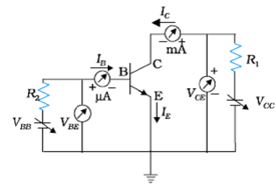
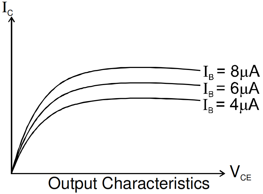
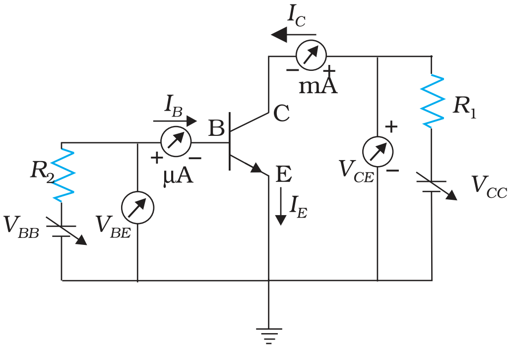
- Draw the circuit diagram for studying the characteristics of a transistor in common emitter configuration. Explain briefly and show how input and output characteristics are drawn.
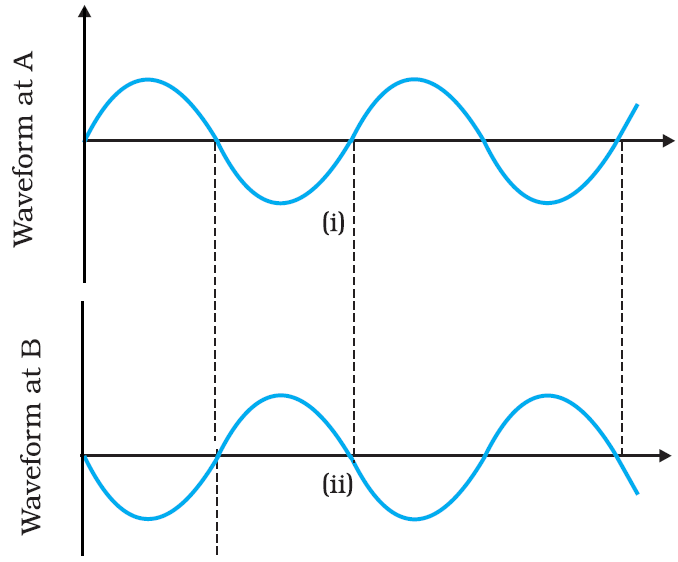
- The figure shows input waveforms A and B to a logic gate. Draw the output waveform for an OR gate. Write the truth table for this logic gate and draw its logic symbol.

Answer
$\text{Collector to emitter voltage}(V_{CE})\text{in volts}$
Alternate answer
Input characteristics:
$(I_B)\text{ }vs (V_{BE})\text{graph keeping}V_{CE}=\text{constant}$
Output characteristics:
$(I_C)VS(V_{CE})\text{graph keeping}\text{ }I_{B}=\text{constant}$
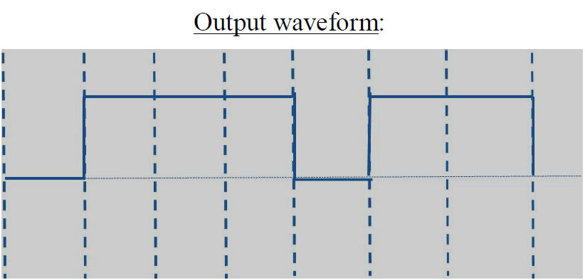
Truth Table:
| Input |
Output |
| A |
B |
Y |
| 0 |
0 |
0 |
| 0 |
1 |
1 |
| 1 |
0 |
1 |
| 1 |
1 |
1 |
Logic symbol:
View full question & answer→Question 143 Marks
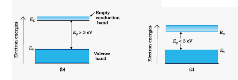
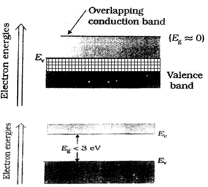
Write any two distinguishing features between conductors, semiconductors and insulators on the basis of energy band diagrams.
Answer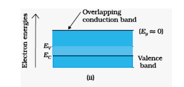
Two distinguishing features:
- In conductors, the valency band and conduction band tend to overlap (or nearly overlap) while in insulators they are seperated by a large energy gap and in semiconductors are separated by a small energy gap.
- The conduction band, of a conductor, has a large number of electrons available for electrical conduction. However the conduction band of insulators is almost empty while that of the semi- conductor has only a (very) small number of such electrons available lectrical conduction.
View full question & answer→Question 153 Marks
- Explain with the help of a diagram formation of depletion region and barrier potential in a $pn$ junction.
- Draw the circuit diagram of a half wave rectifier and explain its working.
Answer
-
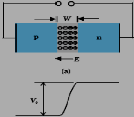
Due to diffusion and drift, the electrons and holes move across the junctions, creating a final stage in which a region is created across the junction wall, which gets devoid of the mobile charge carriers.
This region is called depletion region; The potential difference across the region is called Barriers potential.
-
Working $-$ If an alternating voltage is applied across a diode in series with a load, a pulsating voltage will appear across the load only during that half cycle of the ac input during which the diode is forward biased.
Therefore, in the positive half$-$cycle of ac input there is a current through the load resistor $R_{L,}$ and we get an output voltage whereas half$-$cycle.
There is no output during the negative half cycle.
Thus, the output voltage is restricted to only one direction and is said to be rectified. View full question & answer→Question 163 Marks
For a CE-transistor amplifier, the audio signal voltage across the collector resistance of 2 k$\Omega$ is 2 V. suppose the current amplification factor if the transistor is 100, find the input signal voltage and base current if the base resistance is 1 k$\Omega$.
Answer
- Input signal Voltage:
AC Collector Current- $i_{c} =\frac{\text{V}_{ce}}{\text{R}_{c}} = 1.0 \text{ mA}$
Base Current- $i_{b} =\frac{i_c}{\beta} = \frac{1.0 \text{ mA}}{100} = 0.01 \text{ mA}$
Base signal Voltage= ${i}_{b}\text{R} = 0.01\text{ mA} \times1\text{k}\Omega =10 \text{ mv}$. View full question & answer→Question 173 Marks
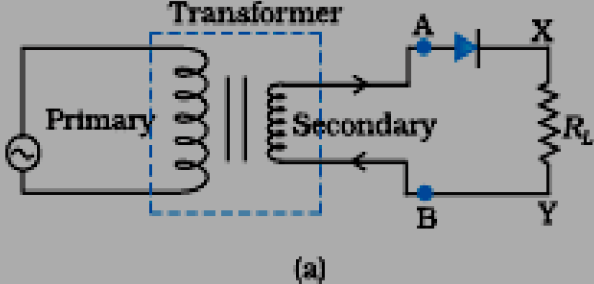
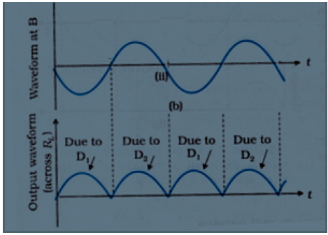
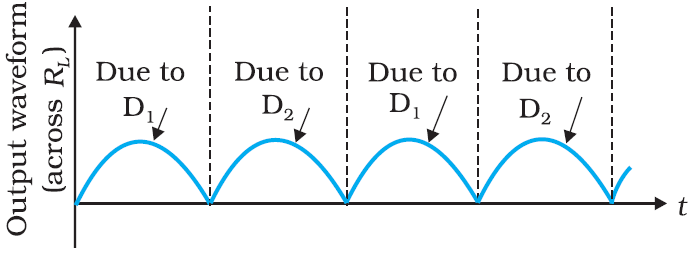
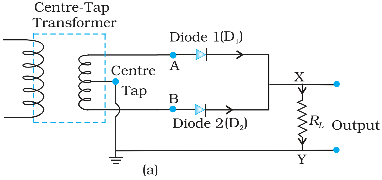
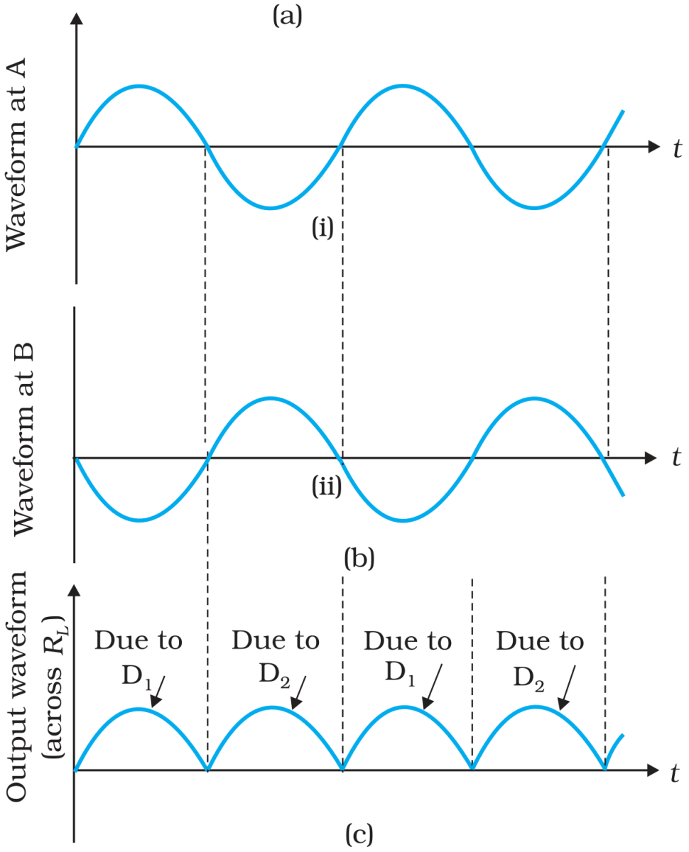
With the help of a circuit diagram, explain the working of a junction diode as a full wave rectifier. Draw its input and output waveforms. Which characteristic property makes the junction diode suitable for rectification?
Answer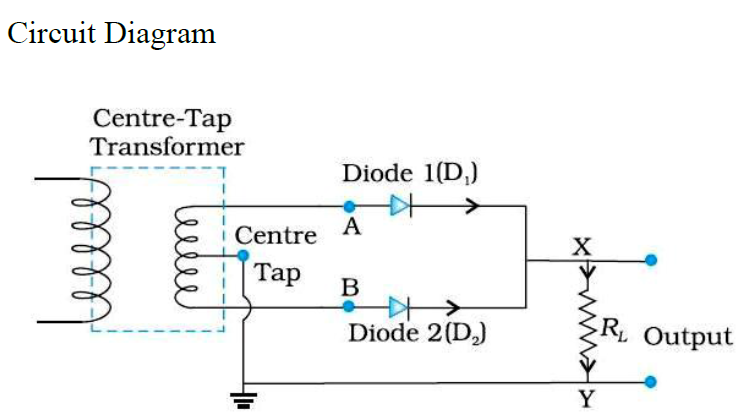
Circuit Diagram
Description of Working$-$ During the positive half of input ac diode $D_1$ get forward bias and $D_2,$ reverse biased and during negative half of input $ac,$ polarity get reversed, $D_2$ get forward bias and $D_1$ reverse bias.
Hence, output is obtained across $R_L$ during entire cycle of $ac.$
Wave forms
Input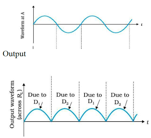
Characteristic property:
Diode allows the current to pass only when it is forward based. View full question & answer→Question 183 Marks
The outputs of two NOT gates are fed to a NOR gate. Draw the logic circuit of the combination of gates. Write its truth table. Identify the gate equivalent to this circuit.
AnswerTo draw the logic circuit:
Truth Table:
| A |
B |
Y |
| 0 |
0 |
0 |
| 1 |
0 |
0 |
| 0 |
1 |
0 |
| 1 |
1 |
1 |
Identification: AND gate.
View full question & answer→Question 193 Marks
- In the following diagram, is the junction diode forward biased or reverse biased?
- Draw the circuit diagram of a full wave rectifier and state how it works.
Answer
- Reverse Biased
- Diagram of full wave rectifier
Working: The diode $D_1$ is forward biased during one half cycle and current flows through the resistor, but diode $D_2$ is reverse biased and no current flows through it.
During the other half of the signal$, D_1$ gets reverse biased and no current passes through it, $D_2$ gets forward biased and current flows through it. In both half cycles current, through the resistor, flows in the same direction.
View full question & answer→Question 203 Marks
- Write the functions of the three segments of a transistor.
- The figure shows the input waveforms A and B for ‘AND’ gate. Draw the output waveform and write the truth table for this logic gate.
Answer
- Emitter: Supplies a large number of majority charge carriers.
Base: Controls the flow of majority carriers from the emitter to the collector.
Collector: It collects the majority carriers from the base/majority of those emitted by the emitter.
-
| Truth Table |
| A |
B |
Y |
| 0 |
0 |
0 |
| 0 |
1 |
0 |
| 1 |
0 |
0 |
| 1 |
1 |
1 |
View full question & answer→Question 213 Marks
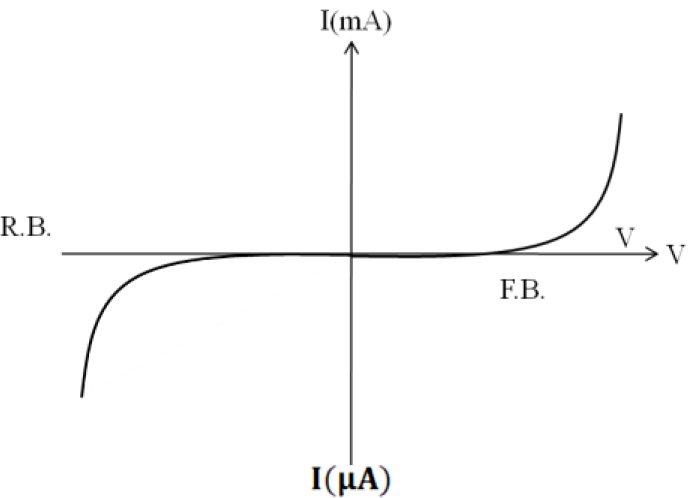
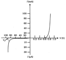
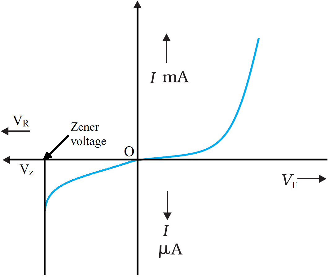
Draw V – I characteristics of a p–n junction diode. Answer the following questions, giving reasons:
- Why is the current under reverse bias almost independent of the applied potential up to a critical voltage?
- Why does the reverse current show a sudden increase at the critical voltage?
Name any semiconductor device which operates under the reverse bias in the breakdown region.
Answer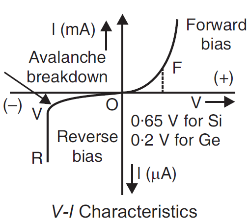
- In the reverse biasing, the current of order of $\mu$ A is due to movement/drifting of minority charge carriers from one region to another through the junction.
A small applied voltage is sufficient to sweep the minority charge carriers through the junction.
So reverse current is almost independent of critical voltage.
- At critical voltage (or breakdown voltage), a large number of covalent bonds break, resulting in the increase of large number of charge carriers. Hence current increases at critical voltage.
Semiconductor device that is used in reverse biasing is zener diode. View full question & answer→Question 223 Marks
In the circuit shown in the figure, identify the equivalent gate of the circuit and make its truth table.
Answer
Gates, P, Q and R act as NOT, NOT and NAND gates respectively.
So
The combination acts as OR Gate.
 Truth Table of OR Gate
| A |
B |
Y |
| 0 |
0 |
0 |
| 1 |
0 |
1 |
| 0 |
1 |
1 |
| 1 |
1 |
1 |
View full question & answer→Question 233 Marks
You are given a circuit below. Write its truth table. Hence, identify the logic operation carried out by this circuit. Draw the logic symbol of the gate it corresponds to.
Answer
| A |
B |
$\text{X} =\overline{\text{A}}$ |
$\text{Y} = \overline{\text{B}}$ |
$\text{Z}=\overline{\bar{\text{A}}+\bar{\text{B}}}=\text{A}\cdot\text{B}$ |
| 0 |
0 |
1 |
1 |
1 |
| 0 |
1 |
1 |
0 |
0 |
| 1 |
0 |
0 |
1 |
0 |
| 1 |
1 |
0 |
0 |
0 |
Logic operation is AND or (A.B)
Logic Symbol
View full question & answer→Question 243 Marks
Draw a labelled diagram of a full wave rectifier circuit. State its working principle. Show the input-output waveforms.
Answer
Principle
pn junction conducts when it is in forward biased and does not do so when it is reverse biased.
View full question & answer→Question 253 Marks
With the help of a suitable diagram, explain the formation of depletion region in a p-n junction. How does its width change when the junction is (i) forward biased, and (ii) reverse biased?
Answer
Formation: During the formation of p-n junction, and due to the concentration gradient across p, and n sides, holes diffuse from p-side to n-side (p → n) and electrons diffuse from n-side to p-side (n → p). This motion of charge carriers gives rise to diffusion current across the junction. When an electron diffuses from n → p, it leaves behind an immobile ionised donor (positive charge) on n-side. As the electrons continue to diffuse from n → p, a layer of positive charge (or positive space-charge region) on n-side of the junction is developed. Similarly, a layer of negative charge (or negative space-charge region) on the p-side of the junction is developed. This space-charge region, developed on either side of the junction is known as depletion region as the electrons and holes taking part in the initial movement across the junction deplete, this region of its free charges.
Width of depletion region layer decreases when the junction is forward biased and increases when it is reversed biased.
View full question & answer→Question 263 Marks
Give a circuit diagram of a common emitter amplifier using an n-p-n transistor. Draw the input and output waveforms of the signal. Write the expression for its voltage gain.
AnswerCircuit diagram:

Input and output waveforms:

The voltage gain of the amplifier is
$\text{A}_{v} = \frac{\text{v}_{0}}{\text{v}_{t}} = \frac{\Delta\text{V}_{CE}}{\text{r}\Delta\text{I}_{B}}$
$ = - \frac{\beta_{ac}\text{R}_{L}}{\text{r}}.$ View full question & answer→Question 273 Marks
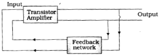
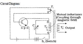
State briefly the underlying principle of a transistor oscillator. Draw a circuit diagram showing how the feedback is accomplished by inductive coupling. Explain the oscillator action.
Question 283 Marks
The inputs A and B are inverted by using two NOT gates and their outputs are fed to the NOR gate as shown below.

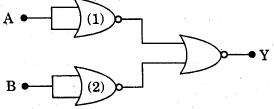
Analyse the action of the gates (1) and (2) and identify the logic gate of the complete circuit so obtained. Give its symbol and the truth table.
AnswerAnalysis: (1) and (2) are ‘NOT’ gates
Identification: Whole circuit is equivalent to AND gate
$(\overline{\overline{\text{A}} + \overline{\text{B}}}) = \text{A}.\text{B}$
Symbol:

Truth table:
| Input |
Output |
| A |
B |
Y |
| 0 |
0 |
0 |
| 0 |
1 |
0 |
| 1 |
0 |
0 |
| 1 |
1 |
1 |
View full question & answer→Question 293 Marks
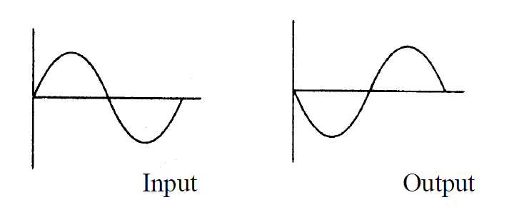
Draw the labelled circuit diagram of a common-emitter transistor amplifier. Explain clearly how the input and output signals are in opposite phase.
AnswerCircuit Diagram:
Explanation: The voltage gain of the amplifier is $\text{A}_{v} = -\beta_{\text{ac}}\text{R}_{L}/\text{r}$
The negative sign represents the output voltage which is opposite in phase with the input voltage, as input voltage increases output voltage decreases.
Graphically:
View full question & answer→Question 303 Marks
Draw the circuit diagram of a common emitter amplifier using $n-p-n$ transistor. What is the phase differnece between the input signal and output voltage? State two reasons why a common emitter amplifier is preferred to a common base amplifier.
AnswerCircuit diagram of $CE$ Amplifier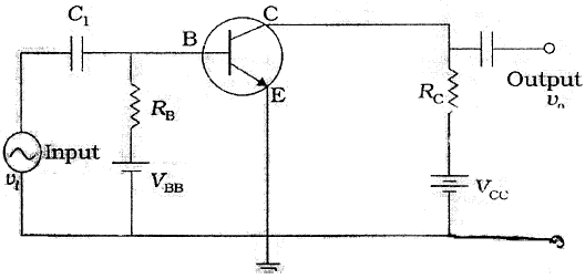
Phase relation between input and output signal is $180^\circ OR \ \pi$ radian. High current gain/cascading is easier$/$high power gain. View full question & answer→Question 313 Marks
Explain the formation of energy band in solids. Draw energy band diagram for (i) a conductor, (ii) an intrinsic semiconductor.
AnswerIsolated atoms have discrete energy levels in a crystal, the presence of large number of closely packed atoms, leads to inter atomic interaction and the energy levels get spread out or broadened into energy bands.
Alternate Answer

View full question & answer→Question 323 Marks
Explain (i) forward biasing, (ii) reverse biasing of a P-N junction diode. With the help of a circuit diagram, explain the use of this device as a half-wave rectifier.
Answer
Forward bias: We apply a voltage v such that n-side is negative and p-side is positive. (Diode conducts current)
Reverse bias: We apply a voltage v such that n-side is positive and p-side is negative. (Diode is cut off)
Alternate Answer
other point relevant to forward bias/reverse bias should also be given full marks. (Explanation with /without circuit diagram)
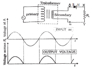
Explanation: When the voltage at A is +ve, the diode is forward biased and it conducts. When A is negative, the diode is reverse biased and its does not conduct. Therefore, in the positive half cycle there is a current through the load resistor and we get an output voltage as shown in figure. But there is negligibly small current in the negative half cycle and hence no output. Thus, the output voltage, though still varying, is restricted to one direction only.
View full question & answer→Question 333 Marks
- Describe the working principle of a solar cell. Mention three basic processes involved in the generation of emf.
- Why are Si and GaAs preferred materials for solar cells?
Answer
- When solar cell is illuminated with light photons of energy $(hv)$ greater than the energy gap $\text{E}_{\text{g}}$ of the semiconductor, then electron hole pairs are generated due to absorption of photons.
The three basic processes involved in the generation of emf:
- Generation of e-h pairs due to light with close to the junction.
- Separation of electrons and holes due to electric field of the depletion region.
- The electrons reaching the n side are collected by the front contact and holes reaching p side are collected by back contact.
- Solar radiation has maximum intensity of photons of energy = 1.5eV.
Hence semiconducting materials Si and GaAs, with band gap $\approx$ 1.5 eV, are preferred materials for solar cells. View full question & answer→Question 343 Marks
Explain briefly with the help of necessary diagrams, the forward and the reverse biasing of a p-n junction diode. Also draw their characteristic curves in the two cases.
Answer
In forward bias, applied voltage does not support potential barrier. As a result, the depletion layer width decreases and barrier height is reduced. Due to the applied voltage, electrons from n side cross the depletion region and reach p side. Similarly holes from p side cross the junction and reach the n side. The motion of charged carriers, on either side, give rise to current. In reverse bias, applied voltage support potential barrier. As a result, barrier height is increased, depletion layer widens. This suppresses the flow of electrons from n → p and holes from p → n. Diffusion current decreases. The electric field direction of the junction is such that if electrons on p side or holes on n side in their random motion comes close to the junction, they will be swept to its majority zone. This drift of carriers give rise to the current called reverse current.
View full question & answer→Question 353 Marks
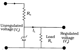
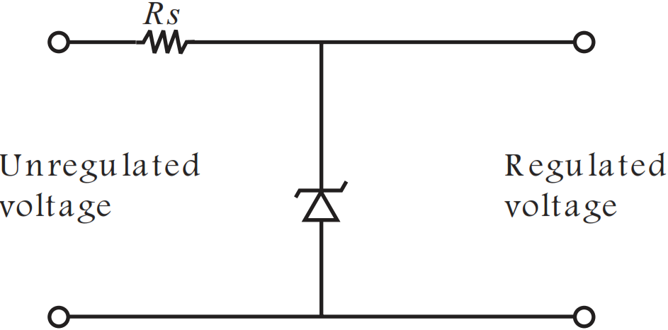
A zener diode is fabricated by heavily doping both $p-$ and $n-$ sides of the junction. Explain, why? Briefly explain the use of zener diode as a de voltage regulator with the help of a circuit diagram.
AnswerBy heavily doping both $p$ and $n$ sides of the junction, depletion region formed is very thin$, i.e. < 10^{-6}$
Hence, electric field, across the junction is very high $( \sim5\times10^{-6}{\text{V/m}})$ even for a small reverse bias voltage. This can lead to a 'breakdown' during reverse biasing.
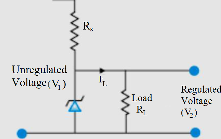
If the input voltage increases/decreases, current through resister $R_{s}$ and Zener diode, also increases/decreases. This increases/decreases the voltage drop across $R_s$ Without any change in voltage across the Zener diode.
This is because, in the breakdown region, Zener voltage remains constant even though the current through the Zener diode changes. View full question & answer→Question 363 Marks
- Write the functions of three segments of a transistor.
- Draw the circuit diagram for studying the input and output characteristics of $n-p-n$ transistor in common emitter configuration. Using the circuit, explain how input, output characteristics are obtained.
Answer
- Emitter: Supplies the large number of majority charge carriers for the flow of current through the transistor.
Base : Controls the movement of charge carriers coming from emitter region.
Collector : Collects a major portion of the majority carriers supplied by the emitter.
Emitter : Heavily doped and of moderate size.
Base : Central region, thin and lightly doped.
Collector : Moderately doped and large sized.
-
Input characteristics are obtained by recording the values of base current $I_B,$ for different values of $V_{BE}$ at constant $V_{CE.}$
Output characteristics are obtained by recording the values of $I_{C}$ for different values of $V_{CE}$ at constant $I_B.$
Alternate Answer
Also, accept input/output characteristic curves. View full question & answer→Question 373 Marks
Draw a circuit diagram of a transistor amplifier in $CE$ configuration.
Define the terms: $(i)$ Input resistance and $(ii)$ Current amplification factor. How are these determined using typical input and output characteristics?
Answer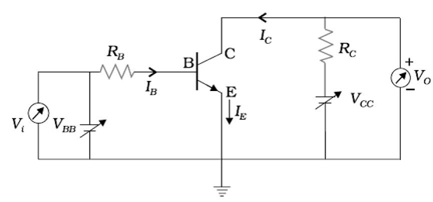
Input resistance
$\text{R}_{i} = \bigg(\frac{\bigtriangleup\text{V}_{BE}}{\bigtriangleup\text{I}_{B}}\bigg)_{V_{CE}}$
Current amplification factor
$\beta_{ac} = \bigg(\frac{\bigtriangleup\text{I}_{c}}{\bigtriangleup\text{I}_{B}}\bigg)_{V_{CE}}$
The value of input resistance is determined from the slope of $IB$ versus $V_{BE}$ plot at constant $V_{BE}.$
The value of current amplification factor is obtained from the slope of collector $I_C$ versus $V_{CE}$ plot using different values of $I_B.$ View full question & answer→Question 383 Marks
With what considerations in view, a photodiode is fabricated? State its working with the help of a suitable diagram.
Eventhough the current in the forward bias is known to be more than in the reverse bias, yet the photodiode works in reverse bias. What is the reason?
AnswerIt is fabricated with a transparent window to allow light to fall on diode.
When the photodiode is illuminated with photons of energy $\ce{(hv > E_g)}$ greater than the energy gap of the semiconductor, electron $-$ holes pairs are generated.
These gets separated due to the junction electric field $($before they recombine$)$ which produces an emf.
Reason: It is easier to observe the change in the current, with change in light intensity, if a reverse bias is applied.
Alternate Answer
The fractional change in the minority carrier current, obtained under reverse bias, is much more than the corresponding fractional change in majority carrier current obtained under forward bias. View full question & answer→Question 393 Marks
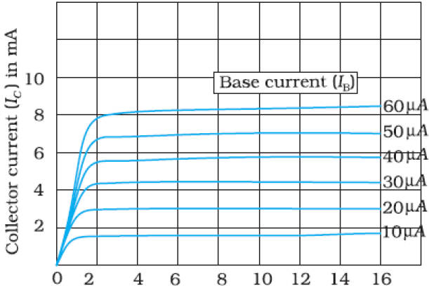
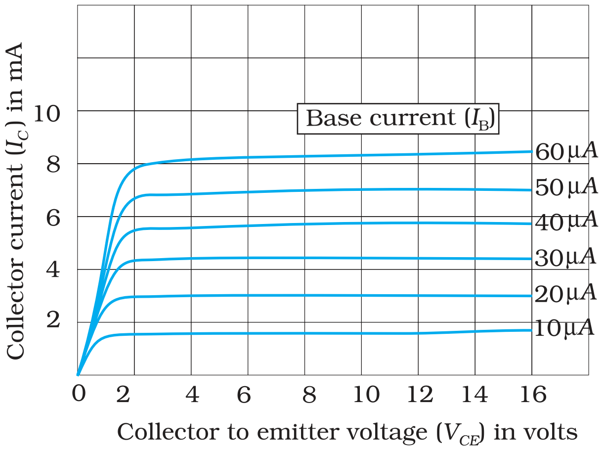
Output characteristics of an $n-p-n$ transistor in $CE$ configuration is shown in the figure. Determine:
- Dynamic output resistance.
- $Dc$ current gain and.
- $Ac$ current gain at an operating point $V_{CE} = 10V,$ when $ I_B =30\mu\ A$.
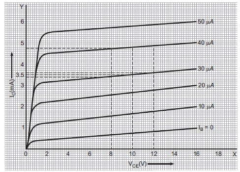
Answer
- Dynamic output resistance is given by
$\text{r}_{o}=\bigg(\frac{\Delta\text{V}_{CE}}{\Delta\text{I}_{c}}\bigg)_{I_{B}}$
For $I_B = 30 \mu \ A, \Delta \text{VCE} = (12 - 8) = 4V$ and $\Delta I_C = (3.6 – 3.4) = 0.2m\ A$
$\therefore\text{r}_{o} = \frac{4\text{V}}{0.2\text{mA}} =\frac{4}{0.2\times10^{-3}} =2 \times10^{4}\text{ohm}$
- dc current gain
$\beta_{dc} = \frac{\text{I}_{c}}{\text{I}_{b}}$
At $V_{CE} = 10V$ and $ I_b = 30\mu\ A,$ the value of $I_c = 3.5m A$
$\beta_{dc} = \frac{3.5\text{mA}}{30\mu\text{A}} = \frac{3.5\times10^{-3}}{30\times10^{-6}}$
$\beta_{dc} = 117$
- ac current gain
$\beta_{dc} = \bigg(\frac{\Delta\text{I}_{C}}{\Delta\text{I}_{B}}\bigg)_{V_{CE}}$
At $V_{CE} =10V, \Delta I_C = (3.5 - 2.5) mA = 1mA$
and $\Delta \ I_b= (30 \mu\ A - 20 \mu\ A) = 10 \mu\ A$
$\therefore\beta_{ac} = \frac{1\mu\text{A}}{10\mu\text{A}} = 100.$ View full question & answer→Question 403 Marks
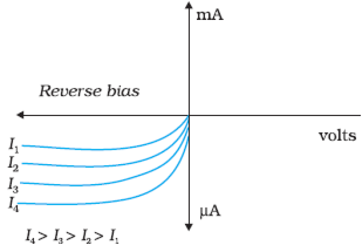
The figure below shows the $\text{V-I}$ characteristic of a semiconductor diode.
- Identify the semiconductor diode used.
- Draw the circuit diagram to obtain the given characteristic of this device.
- Briefly, explain how this diode can be used as a voltage regulator.
Answer
- Zener diode/ $P-N$ junction diode/Semiconductor diode/Silicon diode.
- Circuit diagram $($Either forward bias or reverse bias$)$
Alternate Answer
-
If the input voltage increases, the current through $R_s$ and Zener diode also increases.
This increases voltage drop across $R_s$ without any change of voltage across zenor diode.
Alternate Answer
The semiconductor diode/ $(p-n) $ junction diode can be used as a voltage regulator by increasing its doping level to make it as a Zener diode. View full question & answer→Question 413 Marks
Explain, with the help of a schematic diagram, the principle and working of a Light Emitting Diode. What criterion is kept in mind while choosing the semiconductor material for such a device? Write any two advantages of Light Emitting Diode over conventional incandescent lamps.
Answer 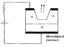 Principle:
When electrons fall from a higher to a lower energy level, containing holes, energy, in the form of light radiation, gets released.
Working:
Criterion:
The semiconductor material used in LED is chosen according to the required wavelength of emitted radiation.
Alternate Answer
Chosen to have a energy gap matching the energy of a photon of the radiation required to be emitted.
Advantages:
- Low operation voltage.
- Less power.
- No warm up time.
- Fast action.
- Light emitted is nearly monochromatic.
- Long life.
View full question & answer→Question 423 Marks
What is an intrinsic semiconductor? How can this material be converted into (1) P-type (2) N-type extrinsic semiconductor? Explain with the help of energy band diagrams.
AnswerIntrinsic semiconductor: Pure semi-conductor having no impurities or negligible impurities.Conversion into –
- P-type – by doping with small amount of trivalent impurities.
- N-type- by doping with small amount of pentavalent impurity.
View full question & answer→Question 433 Marks
Draw a circuit diagram for use of NPN transistor as an amplifier in common emitter configuration. The input resistance of a transistor is $1000 \Omega$. On changing its base current by $10\mu\text{A}$ the collector current increases by 2mA. If a load resistance of $5\text{K}\Omega$. Is used in the circuit, calculate:
- The current gain.
- Voltage gain of the amplifier.
Answer
- Circuit Diagram
- Current Gain $\big(\beta\big) = \frac{\bigtriangleup\text{I}_{c}}{\bigtriangleup\text{I}_{b}}$
$=\frac{2\times10^{-3}}{10\times10^{-6}}=200$
- Voltage Gain $=\beta\times\frac{r_\circ}{r_1} $
$ =200\times\frac{5\times10^{3}}{1000} = 1000.$ View full question & answer→Question 443 Marks
- A student wants to use two $p-n$ junction diodes to convert alternating current into direct current. Draw the labelled circuit diagram she would use and explain how it works.
- Give the truth table and circuit symbol for $\text{NAND}$ gate.
Answer
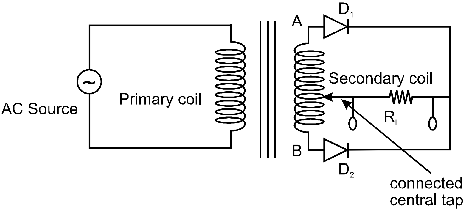
- Working:
- For $+ve$ half cycle of $AC$ source, let $A$ be at $+ve$ potential and $B$ and $ve$ potential,
- So $, D_1$ will be forward biased and $D_2$ will be reversed biased. Itmeans currentwill only flow through $D_1$ and current will not flow through $D_2$.
- Output is obtained across $R_L.$
- For $-ve$ half cylce $, B$ will be at $+ve$ potential and point $A$ at $ve$ potential,
- So $, D_1$ will be reversed biased and $D_2$ will be forward biased Itmeans that current will only flow through $D_2$ and not through $D_1,$ output is obtained across $R_L$.
- This process is called full wave rectification and the device is called full wave rectifier.
- Truth Table:
Logic Symbol:
View full question & answer→Question 453 Marks
Draw the typical input and output characteristics of an $\text{n - p - n}$ transistor in $CE$ configuration. Show how these characteristics can be used to determine
$(a)$ the input resistance $(r_i),$ and
$(b)$ current amplification factor $(\beta).$
Answer
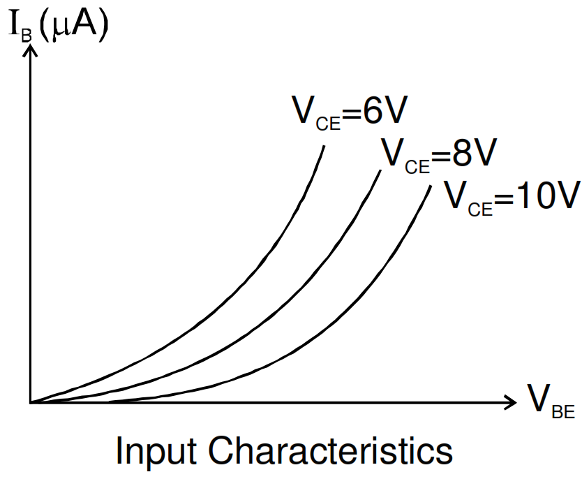
The input resistance $r_i $ of the transistor in $CE$ configuration is defined as the ratio of the small change in base $-$ emitter voltage to the corresponding small change in the base current, when the collector $-$ emitter voltage is kept fixed.
Thus,
$\text{r}_{\text{i}}=\Big[\frac{\Delta\text{V}_{\text{BE}}}{\Delta\text{I}_{\text{B}}}\Big]_{\text{V}_{\text{CE}}=\text{constant}}$
As input characteristic is non $-$ linear, so $r_i$ varies.
At any point of the curve $, r_i$ is equal to the slope of the tangent to the curve.
Current amplification factor $(\beta)$: It is defined as the ratio of the change in collector current to the small change in base current at constant collector $-$ emitter voltage $(V_{CE})$ when the transistor is in the active state.
$\beta_{\text{ac}}=\Big[\frac{\Delta\text{I}_{\text{C}}}{\Delta\text{I}_{\text{B}}}\Big]_{\text{V}_{\text{CE}}=\text{constant}}$
This is also known as small signal current gain and its value is very large. View full question & answer→Question 463 Marks
Give reasons for each of the following:
- The intensity of light at some points on the screen in Young’s double slit experiment is zero.
- The intensity of light transmitted by a polaroid is less than the intensity of the unpolarised light incident on it.
- In the single slit diffraction experiment, some coloured fringes around the central white maximum are observed on the screen when one uses a source of white light.
Answer
- The points where the two waves meet out of phase or with the path difference of an integral multiple of $\frac{\lambda}{2},$ they cancel out the contribution of each other. Alternatively
Due to the destructive interference of two waves.
- When light is passed through a polaroid the vibrations of electric field vector which are perpendicular to the pass axis of the polaroid are absorbed and only those parallel to pass axis pass, therefore the intensity of transmitted light is less than that of the incident light.
- At any point away from the central bright fringe, path difference is different for different colours, therefore maxima for different colours are formed at different points and coloured fringes are seen.
View full question & answer→Question 473 Marks
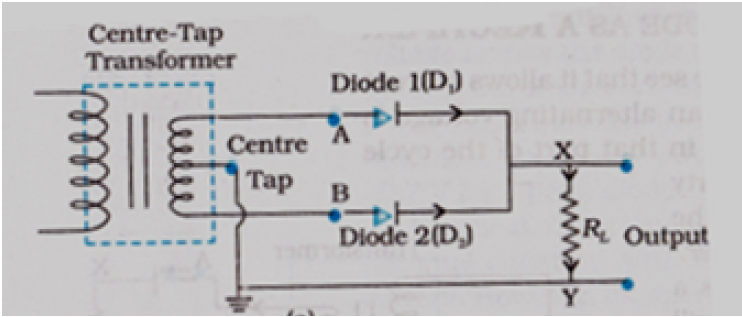
Draw the circuit diagram of a full wave rectifier using two $p-n$ junction
diodes. Explain its working and show input and output voltage variations.
Answer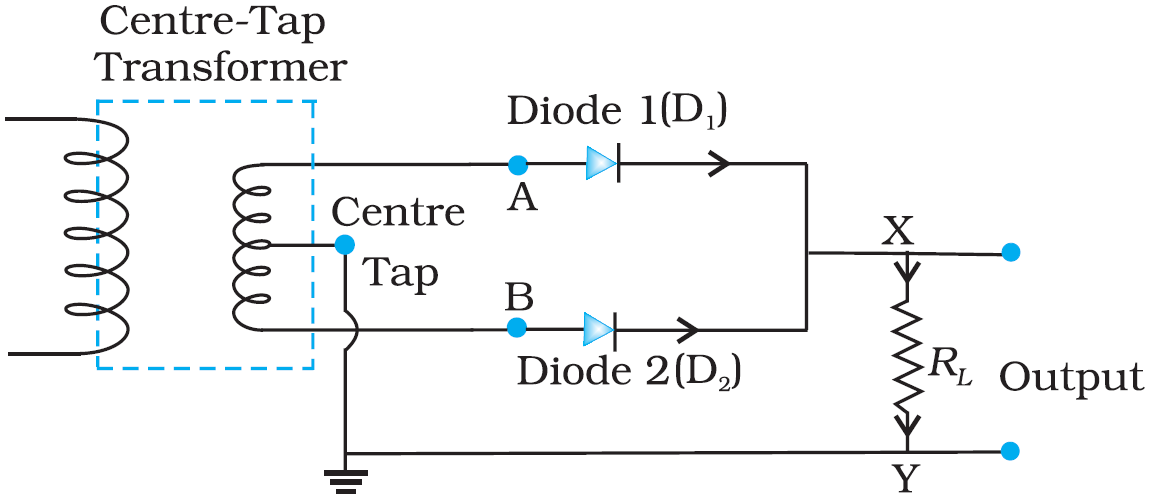
For $+ve$ half cycle of $AC$ input, terminal $A$ or transformer $T$ will be as low voltage relative centre tap terminal $C B$ at high voltage.
So, $D^1$ will be reverse biased $D^2$ will be forward biased.
Diode $D^2$ conducts to give an output across $RL$ through $M$.
For $–ve$ half cycle of input $AC, A$ will be at high voltage $B$ will be at low voltage to make $D^1$ forward and $D^2$ reverse biased. $D^1$ conducts to give an output across $RL$ with same polarity. View full question & answer→Question 483 Marks
- Describe briefly the functions of the three segments of $\text{n-p-n}$ transistor.
- Draw the circuit arrangement for studying the output characteristics of $\text{n-p-n}$ transistor in $CE$ configuration. Explain how the output characteristics is obtained.
Answer
- Three segments of transistor :
- Emitter :
- Segment is on one side of the transistor. It is of moderate size and heavily doped. It supplies a huge number of majority carriers for the current flow through the transistor.
- Base : It is the central segment. It is very thin and lightly doped.
- Collector : It collects a major portion of the majority carrier supplied by the emitter. It is moderately doped and large in size compared to emitter.
- Circuit arrangement for studying the output characteristics of $\text{n-p-n}$ transistor in $CE$ configuration.
Variation of collector current $I_C$ with the collector $-$ Emitter voltage $V_{CE}$ is called output characteristics.
Output characteristics :
The output characteristics describe the relationship between output current $(I_C)$ and output voltage $(V_{CE}).$
First, draw a vertical line and a horizontal line.
The vertical line represents $y-$ axis and horizontal line represents $x-$ axis.
The output current or collector current $(I_C)$ is taken along the $y-$ axis $($vertical line$)$ and the output voltage $(V_{CE})$ is taken along the $x-$ axis $($horizontal line$)$.
To determine the output characteristics, the input current or base current $I_B$ is kept constant at $0 \mu A$ and the output voltage $V_{CE}$ is increased from zero volts to different voltage levels.
For each level of the output voltage, the corresponding output current $(I_C)$ is recorded.
$A$ curve is then drawn between output current $I_{C }$ and output voltage $V_{CE}$ at constant input current $I_B (0 \mu\text{A}).$ View full question & answer→Question 493 Marks
With the help of a simple diagram, explain the working of a silicon solar cell, giving all three basic processes involved. Draw its $I-V$ characteristic.
Answer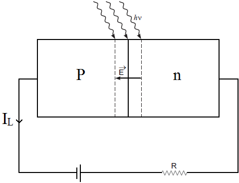
When solar radiations are incident near the depletion layer of solar cell, covalent bonds break absolving the photons to create $e^-$ hole pairs and following three important process occur.
- Generation of $e - h$ pair by breaking of covalent bonds absorbing radiations incident on depletion layer when $hv > Eg.$
- separation of $e^-$ and hole in $n-$ side and holes in $p-$ side to develop a photovoltage $\text{V}$ propto across the solar cell.
- Collection of electrons reaching the $n-$ side by the front contact and holes reaching the pside by the back contact.
$I-V$ characteristics.
Thus the $p-$ side become positive and the $n-$ side becomes negative giving rise to photo voltage. 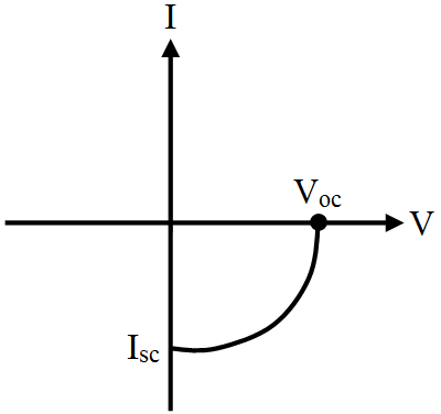
View full question & answer→Question 503 Marks
- Draw circuit diagram and explain the working of a zener diode as a dc voltage regulator with the help of its I-V characteristic.
- What is the purpose of heavy doping of p- and n-sides of a zener diode?
Answer
- Zener diode as a Voltage Regulator.
The Zener diode makes its use as a voltage regulator due to the following property:
When a Zener diode is operated in the breakdown region, the voltage across it remains practically constant for a large change in the current.
A simple circuit of a voltage regulator using a Zener diode is shown in the figure. The Zener diode is connected across load such that it is reverse biased.
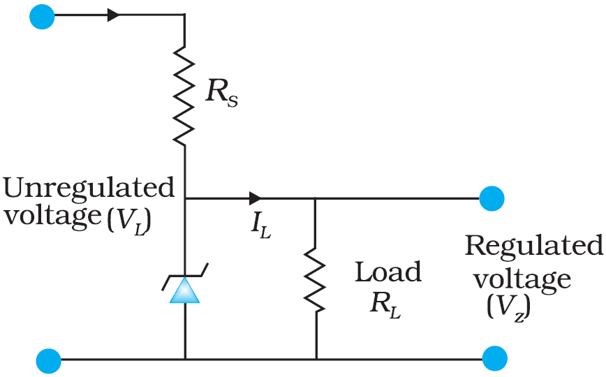
The series resistance R absorbs the output voltage fluctuations so as to maintain constant voltage across the load.
If the input dc voltage increases, the current through R and Zener diode also increases. So, voltage drop across R increases, without any change in the voltage across zener diode.
I-V Characteristics,
- The Zener diode as fabricated by heavily doping both p and n sides of the junction so as to:
- Push the conduction band very near to Fermi level.
- Make depletion layer narrower.
- Making resistance lower and allow a large current to flow with little potential difference.
View full question & answer→Question 513 Marks
- Three photo diodes $D_1 , D_2$ and $D_3$ are made of semiconductors having band gaps of $2.5eV, 2eV$ and $3eV$ respectively. Which of them will not be able to detect light of wavelength $600\ nm$?
- Why photodiodes are required to operate in reverse bias? Explain.
Answer
- Energy of the incident light
$\text{E}=\frac{\text{hC}}{\lambda}$
$=\frac{(6.6\times10^{-34})\times(3\times10^8)}{(600\times10^{-9})\times(1.6\times10^{-19})}$
$\text{E}=2.06\ \text{eV}$
The incident radiations can be detected by a photodiode if the energy of incident radiation photon is greater than the band gap.
This is true only for $D_{2 }(2eV)$.
Hence, only $D_2$ will detect the light of $600\ nm$ wavelength.
- The photodiode is reverse biased for operating in the photoconductive mode. As the photodiode is in reverse bias, the width of the depletion layer increases. This reduces the junction capacitance and thereby the response time. In effect, the reverse bias causes faster response times for the photodiode. The photocurrent is linearly proportional to the illuminance.
View full question & answer→Question 523 Marks
Draw the circuit diagram of a full wave rectifier and explain its working. Also, give the input and output waveforms.
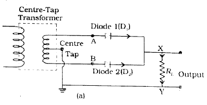
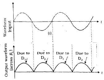
AnswerFull$-$wave rectifier:
Two diodes are used to give rectified $O/ P$ corresponding to both positive as well as negative half cycles.
When the voltage at $A$ with respect to the center tap is positive, and the voltage at $B$ is negative.
Then$, D_1$ is forward biased and $D_2$ is reversed biased.
Hence$, D_1$ conducts and $D_2$ does not.
When the voltage of $A$ becomes negative, then $B$ becomes $+ve$.
Therefore$, D_1$ does not conduct and $D_2 $conducts.
Hence, we obtain output voltage during both the positive as well as negative half of the cycle.
Input and Output waveforms are shown below.
View full question & answer→Question 533 Marks
The following table gives the output of a two input logic gate.
- Identify the logic gate and draw its logic symbol.
- If the output of this gate is fed as input to a NOT gate, name the new logic gate so formed.
|
A
|
B
|
Y
|
|
0
|
0
|
1
|
|
1
|
0
|
1
|
|
0
|
1
|
1
|
|
1
|
1
|
0
|
Answer
The truth table given represents a NAND gate.
Clearly resulting gate will be an AND gate.
Truth table of new gate formed,
| Input |
Output |
| A |
B |
Y |
$\bar{\text{Y}}=\text{Z}$ |
| 0 |
0 |
1 |
0 |
| 0 |
1 |
1 |
0 |
| 1 |
0 |
1 |
0 |
| 1 |
1 |
0 |
0 |
View full question & answer→Question 543 Marks
A Zener of power rating $1W$ is to be used as a voltage regulator. If zener has a breakdown of $5V$ and it has to regulate voltage which fluctuated between $3V$ and $7V,$ what should be the value of $Rs$ for safe operation $($Fig.$)$?
AnswerAccording to the problem, power $= 1W$
Zener breakdown voltage$, V_z = 5V$
Minimum voltage$, V_{min} = 3V$
Maximum voltage$, V_{max} = 7V$
So current $\text{I}_{\text{Z}_\text{max}}=\frac{\text{P}}{\text{V}_\text{Z}}=\frac{1}{5}=0.2\text{A}$
For safe operation $Rs$ will be equal to
$\text{R}_\text{s}=\frac{\text{V}_\text{max}-\text{V}_\text{z}}{\text{I}_{\text{Z}_\text{mzx}}}=\frac{7-5}{0.2}=\frac{2}{0.2}=10\Omega$
View full question & answer→Question 553 Marks
A change of 0.2mA in the base current causes a change of 5mA in the collector current for a common emitter amplifier.
- Find the ac current gain of the transistor.
- If the input resistance is $2\text{k}\Omega$ and its voltage gain is 75, calculate the load resistor used in the circuit.
Answer
- Ac current gain, $\beta=\frac{\Delta\text{I}_\text{C}}{\Delta\text{I}_\text{E}}=\frac{5\text{mA}}{0.2\text{mA}}=25$
- Voltage gain, $\text{A}_\text{V}=\beta\frac{\text{R}_\text{L}}{\text{R}_\text{i}}$
Load resistance $\text{R}_\text{L}=\frac{\text{A}_\text{v}\text{R}_\text{i}}{\beta}$
$=\frac{75\times2\times10^3}{25}$
$=60\times10^3\Omega=6\text{k}\Omega$ View full question & answer→Question 563 Marks
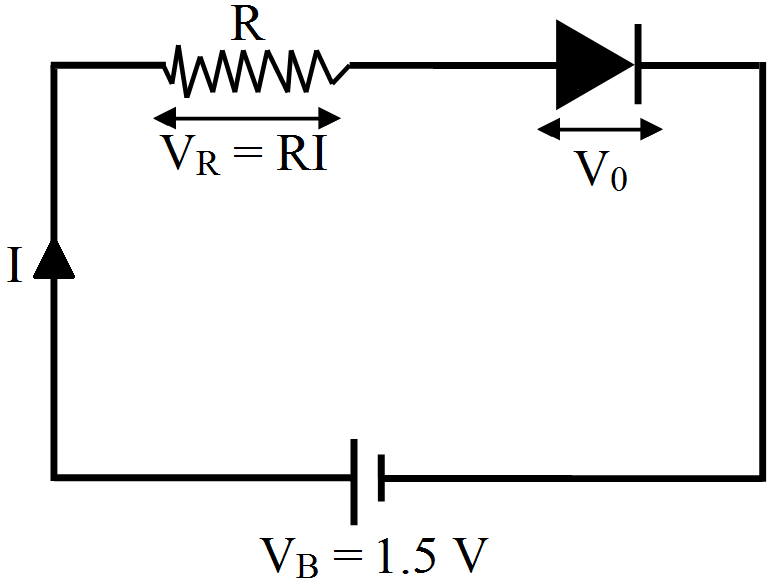
A p-n junction germanium diode when forward biased has a drop of 0.3V which is assumed to be independent of current. The current in excess of 10mA through the diode produces a large Joule-heating which damages (burns) the diode. If we want to use a 1.5V battery to forward-bias the diode, what should be the value of resistor used in series with the diode, so that the maximum current does not exceed 6mA?
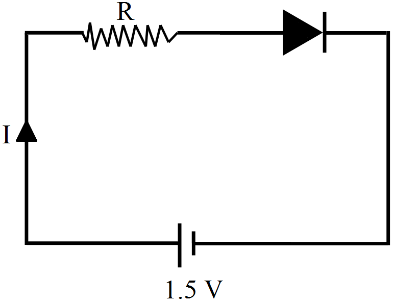
AnswerThe basic equation of diode-circuit is:
$\text{RI}+\text{V}_0=\text{V}_\text{B}$
$\Rightarrow\text{R}=\frac{\text{V}_\text{E}-\text{V}_0}{\text{I}}$
Here, $\text{V}-\text{B}=1.5\text{V},\text{V}_0$
$=0.3\text{V},\text{I}=5\text{mA}=6\times10^{-3}\text{A}$
$\therefore\text{R}=\frac{1.5-0.3}{6\times10^{-3}}$
$=\frac{1.2\times10^{3}}{6}$
$=0.2\times10^3\Omega$
$=200\Omega$
View full question & answer→Question 573 Marks
For the transistor circuit shown in Fig, evaluate $V_E, R_B, R_E$ given $I_C = 1 mA, V_{CE} = 3V, V_{BE} = 0.5 V$ and $V_{CC} = 12 V, \beta = 100.$
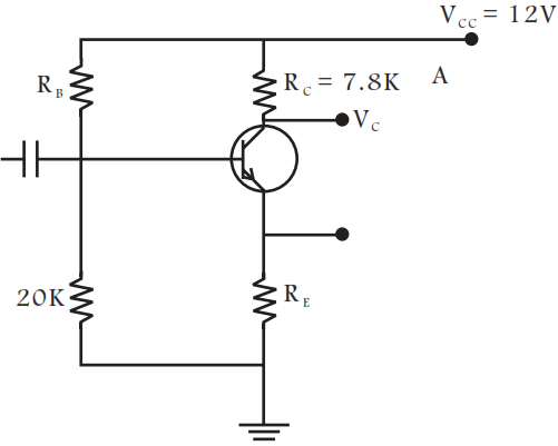
AnswerAs, $I_C ≈ I_E$
$\therefore IC (RC + RE) + VCE = 12V$
$RE = 9 - RC = 1.2K\Omega$
$\therefore VE = 1.2V$
$V_B = V_E + V_{BE} = 1.7V$
$\text{I}=\frac{\text{V}_\text{B}}{20\text{K}}=0.085\text{mA}$
$\text{R}_\text{B}=\frac{12-1.7}{\frac{\text{I}_\text{c}}{\beta}+0+085}$
$=\frac{10.3}{0.01+0.085}$
$=108\text{k}\Omega$
View full question & answer→Question 583 Marks
Indium antimonide has a band gap of 0.23eV between the valence and the conduction band. Find the temperature at which kT equals the band gap.
Answer$\text{E} = 0.23\text{eV, K} = 1.38 \times 10^{-23}$
$\text{KT}=\text{E}$
$\Rightarrow 1.38 \times 10^{-23} \times \text{T} = 0.23 \times 1.6 \times 10^{-19}$
$\Rightarrow\text{T}=\frac{0.23\times1.6\times10^{-19}}{1.38\times10^{-23}}=\frac{0.23\times1.6\times10^4}{1.38}$
$=0.2676\times10^4=2670$
View full question & answer→Question 593 Marks
The band gap for silicon is 1.1eV.
- Find the ratio of the band gap to kT for silicon at room temperature 300K.
- At what temperature does this ratio become one tenth of the value at 300K?
(Silicon will not retain its structure at these high temperatures.)
AnswerBandgap $=1.1\text{eV},\text{T}=300\text{K}$
- Ratio $=\frac{1.1}{\text{KT}}=\frac{1.1}{8.62\times10^{-5}\times3\times10^2}=42.53=43$
- $4.253'=\frac{1.1}{8.62\times10^{-5}\times\text{T}}$ or $\text{T}=\frac{1.1\times10^5}{4.253\times8.62}=3000.47\text{K}.$
View full question & answer→Question 603 Marks
In a $p-n$ junction, the depletion region is $400\ nm$ wide and an electric field of $5 \times 10^5\ V/m$ exists in it.
- Find the height of the potential barrier.
- What should be the minimum kinetic energy of a conduction electron which can diffuse from the $n-$side to the $p-$side?
AnswerLet,
Depletion region width, $\text{d}=400\text{nm}=4\times10^{-7}\text{m}$
Electric field, $\text{E}=5\times10^5\text{Vm}$
Let the potential barrier be $V$.
The relation between the potential and the electric field is given by $V = Ed$
$\Rightarrow\text{V}=\text{E}\times\text{d}=5\times\text{d}$
$\Rightarrow\text{V}=5\times10^5\times4\times10^{-7}=0.2\text{V}$
To find: Kinetic energy required
Energy of any electron accelerated through a potential of $V = eV$
Also, the minimum energy of the electron should be equal to the band gap of the material.
$\therefore$ Potential barrier $\times \ e = 0.2\ eV\ (e =$ Charge of the electron$).$
View full question & answer→Question 613 Marks
The potential barrier existing across an unbiased $p-n$. junction is $0·2$ volt. What minimum kinetic energy a hole should have to diffuse from the $p-$side to the $n-$side if,
- The junction is unbiased.
- The junction is forwardbiased at $0.1$ volt.
- The junction is reverse-biased at $0.1$ volt?
AnswerPotential barrier $= 0.2$ Volt
- $K.E. = \ ($Potential difference$)\ \times\ e = 0.2\ eV ($in unbiased cond$^n)$
- In forward biasing
$KE + Ve = 0.2e$
$\Rightarrow KE = 0.2e - 0.1e = 0.1e.$
- In reverse biasing
$KE - Ve = 0.2e$
$\Rightarrow KE = 0.2e + 0.1e = 0.3e.$ View full question & answer→Question 623 Marks
In a p-n junction, a potential barrier of 250meV exists across the junction. A hole with a kinetic energy of 300meV approaches the junction. Find the kinetic energy of the hole when it crosses the junction if the hole approached the junction.
- From the p-side.
- From the n-side.
AnswerPotential barrier ‘d’ = 250meV
Initial KE of hole = 300meV
We know: KE of the hole decreases when the junction is forward biased and increases when reverse blased in the given ‘Pn’ diode.
So,
- Final KE = (300 - 250)meV = 50meV.
- Initial KE = (300 + 250)meV = 550meV.
View full question & answer→Question 633 Marks
In a common emitter mode of a transistor, the d.c. current gain is 20, the emitter current is 7mA. Calculate (i) base current and (ii) collector current.
AnswerGiven, $\beta=20,\text{i}_\text{E}=7\text{mA}$
- $\beta=\frac{\text{i}_\text{C}}{\text{i}_\text{B}}=\frac{\text{e}_\text{E}-\text{i}_\text{B}}{\text{i}_\text{B}}$ or $\beta_{\text{i}_\beta}=\text{i}_\text{E}=\text{i}_\text{B}$
$\Rightarrow\text{i}_\text{B}=\frac{\text{i}_\text{E}}{\beta+1}$
$=\frac{7\text{mA}}{20+1}=\frac{7}{21}\text{mA} $
$=\frac13\text{mA}$
- $\text{i}_\text{C}=\text{i}_\text{E}-\text{i}_\text{B}=7-\frac13=\frac{20}{3}\text{mA}$
View full question & answer→Question 643 Marks
In a silicon transistor, the base current is changed by $20\mu\text{A}.$ This results in a change of $0.02V$ in base to emitter voltage and a change of $2m\ A$ in the collector current.
- Find the input resistance, $\beta- ac$ and trans conductance of the transistor.
- This transistor is used as an amplifier in $CE$ configuration with a load resistance $5\text{k}\Omega$ What is the voltage gain of the amplifier?
AnswerGiven $\Delta\text{I}_\text{B} = 20\mu\text{A} = 20 \times 10^{-3}\text{mA} = 0.020\text{m A,}$
$\Delta\text{V}_\text{BE} = 0.02\text{V}, \Delta\text{I}_\text{C} = 2\text{mA}$
Input resistance, $\text{R}_\text{i}=\frac{\Delta\text{V}_\text{BE}}{\Delta\text{I}_\text{B}}=\frac{ 0.02}{20\times10^{-6}}\Omega=10^3\Omega=1\text{k}\Omega$
Current gain, $\beta_\text{ac}=\frac{\Delta\text{I}_\text{C}}{\Delta\text{I}_\text{B}}=\frac{\text{2mA}}{0.020\text{mA}}=100$
Trans conductance of a transistor is defined as the ratio of change in collector current to the change in base to emitter voltage at constant collector to emitter voltage, i.e.,
$\text{gm}=\Big(\frac{\Delta\text{I}_\text{C}}{\Delta\text{V}_\text{BE}}\Big)_{\text{V}_\text{CE} =\text{cons}\tan}\text{t}=\frac{2\times10^{-3}}{0.02}=0.1\text{W}^{-1}$
Voltage gain, $\text{A}_\text{v}=\frac{\text{R}_\text{L}}{\text{R}_\text{i}}\times\beta$
Given $\text{RL}=5\text{k}\Omega=5\times103\Omega,$
$\therefore\text{A}_\text{v}=\frac{5\times10^3}{1000}\times1000=500$
As $CE$ amplifier causes a phase shift of $180^\circ$ between input and output voltages,
So voltage gain $, A_ν = -500.$
View full question & answer→Question 653 Marks
Estimate the proportion of boron impurity whieh will increase the conductivity of a pure silicon sample by a factor of $100$. Assume that each boron atom creates a hole and the concentration of holes in pure silicon at the same temperature is $7 \times 10^{15}$ holes per cubic metre. Density of silicon is $5 \times 10^{21}$ atoms per cubic metre.
AnswerTotal no.of charge carriers initially $=2\times7\times10^{15}=14\times10^{15}$ Cubic meter.
Finally the total no.of charge carriers $=14\times10^{17}\text{m}^3$
We know,
The product of the concentrations of holes and conduction electrons remains, almost the same.
Let $x$ be the no.of holes.
So, $\big(7\times10^{15}\big)\times\big(7\times10^{15}\big)=\text{x}\times\big(14\times10^{17}-\text{x}\big)$
$\Rightarrow14\text{x}\times10^{17}-\text{x}^2=79\times10^{30}$
$\Rightarrow\text{x}^2-14\text{x}\times10^{17}-49\times10^{30}=0$
$\text{x}=\frac{14\times10^{17}\pm14^2\times\sqrt{10^{34}+4\times49\times10^{30}}}{2}$ $=14.00035\times10^{17}.$
$=$ Increased in no. of holes or the no.of atoms of Boron added.
$\Rightarrow 1$ atom of Boron is added per $\frac{5\times10^{28}}{1386.035\times10^{15}}$ $=3.607\times10^{-3}\times10^{13}$
$=3.607\times10^{10}.$
View full question & answer→Question 663 Marks
If each diode in Fig. has a forward bias resistance of $25\Omega$ and infinite resistance in reverse bias, what will be the values of the current $I_1, I_2, I_3$ and $I_4$?
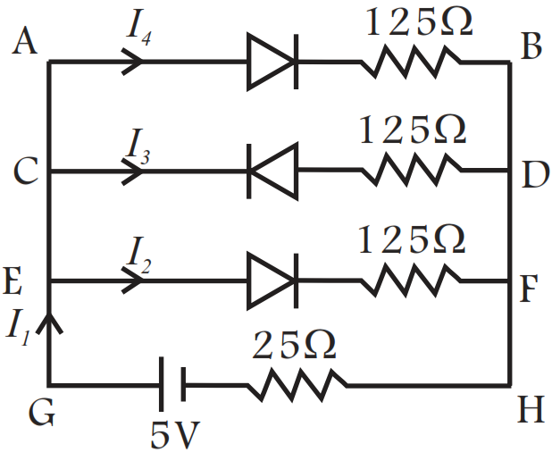
Answer$I_3$ is zero as the diode in that branch is reverse, so,
Resistance in branch $AB = 25 + 125 = 150\Omega , ($let $R_1)$
Resistance in branch $EF = 25 + 125 = 150\Omega . ($let$ R_2)$
As $AB$ and $EF$ are identical parallel branches, their effective resistance is $150/2 = 75\Omega .$
Net resistance in the circuit $= (75 + 25) = 100W .$
Now, Current $I_1 = 5/100 = 0.05A$
As resistances of $AB$ and $EF$ are equal, and $I_1 = I_2 + I_3 + I_4, I_3 = 0$
So, $I_2 = I_4 = 0.025A.$
View full question & answer→Question 673 Marks
In a pure semiconductor, the number of conduction electrons is $6 \times 10^{19}$ per cubic metre. How many holes are there in a sample of size $1\ cm \times 1\ cm \times 1mm$?
AnswerIn a pure semiconductor, the no. of conduction electrons $=$ no. of holes
Given volume $=1\text{cm}\times1\text{cm}\times1\text{mm}$
$=1\times10^{-2}\times1\times10^{-2}\times1\times10^{-3}=10^{-7}\text{m}^3$
No.of electrons $=6\times10^{19}\times10^{-7}=6\times10^{12}$
Hence no.of holes $=6\times10^{12}$
View full question & answer→Question 683 Marks
The conductivity of a pure semiconductor is roughly proportional to $\text{T}^\frac{3}{2}\text{e}^{\frac{-\Delta\text{E}}{2\text{kT}}}$ where $\Delta\text{E}$ is the band gap. The band gap for germanium is 0.74eV at 4K and 0.67eV at 300K. By what factor does the conductivity of pure germanium increase as the temperature is raised from 4K to 300K?
Answer$\sigma=\text{T}^\frac{3}{2}\text{e}^\frac{-\Delta\text{E}}{2\text{KT}}\text{ at }4^\circ\text{K}$
$\sigma=4^\frac{3}{2}=\text{e}^{\frac{-0.67}{{2\times8.62\times10^{-5}\times4}}}=8\times\text{e}^{-1073.08}$
$\text{At } 300\text{K},$
$\sigma=300^\frac{3}{2}\text{ e}^{\frac{-0.67}{{2\times8.62\times10^{-5}\times300}}}=\frac{3\times1730}{8}\text{e}^{-12.95}$
$\text{Ratio}=\frac{8\times\text{e}^{-1073.08}}{\Big[\frac{3\times1730}{8}\Big]\times\text{e}^{-12.95}}=\frac{64}{3\times1730}\text{e}^{-1060.13}$
View full question & answer→Question 693 Marks
The band gap between the valence and the conduction bands in zinc oxide (ZnO) is 3.2eV. Suppose an electron in the conduction band combines with a hole in the valence band and the excess energy is released in the form of electromagnetic radiation. Find the maximum wavelength that can be emitted in this process.
AnswerGiven:
Band gap = 3.2eV
As the electron in the conduction band combines with the hole in the valence band, the minimum energy band gap (because maximum energy is released) through which the electron has to jump will be equal to the band gap of the material.
This implies that the maximum energy released in this process will be equal to the band gap of the material.
Here,
$\text{E}=3.2\text{eV}$
Thus,
$\Rightarrow3.2\text{eV}=\frac{1242\text{eV}-\text{nm}}{\lambda}$
$\Rightarrow\lambda=388.1\text{nm}$
View full question & answer→Question 703 Marks
The product of the hole concentration and the conduction electron concentration turns out to be independent of the amount of any impurity doped. The concentration of conduction electrons in germanium is $6 \times 10^{19 }$ per cubic metre. When some phosphorus impurity is doped into a germanium sample, the concentration of conduction electrons increases to $2 \times 10^{23}$ per cubic metre. Find the concentration of the holes in the doped germanium.
Answer$($No. of holes$) ($No.of conduction electrons$) =$ constant.
At first:
No. of conduction electrons $= 6 \times 10^{19}$
No. of holes $= 6 \times 10^{19}$
After doping
No. of conduction electrons $= 2 \times 10^{23}$
No. of holes $= x.$
$\big(6\times10^{19}\big)\big(6\times10^{19}\big)=(2\times10^{23}\big)\text{x}$
$\Rightarrow\frac{6\times6\times10^{19+19}}{2\times10^{23}}=\text{x}$
$\Rightarrow\text{x}=18\times10^{15}=1.8\times10^{16}.$
View full question & answer→Question 713 Marks
Sn, C, and Si, Ge are all group XIV elements. Yet, Sn is a conductor, C is an insulator while Si and Ge are semiconductors. Why?
AnswerThe conduction level of any element depends on the energy gap between its conduction band and valence band.
In conductors, there is no energy gap between conduction band and valence band. For insulator, the energy gap is large and for semiconductor the energy gap is moderate.
The energy gap for Sn is 0eV, for C is 5.4eV, for Si is 1.1eV and for Ge is 0.7eV related to their atomic size. Therefore Sn is a conductoc, C is an insulator, and Ge and Si are semiconductors.
View full question & answer→Question 723 Marks
A semiconducting material has a band gap of 1eV. Acceptor impurities are doped into it which create acceptor levels 1meV above the valence band. Assume that the transition from one energy level to the other is almost forbidden if kT is less than $\frac{1}{50}$ of the energy gap. Also, if kT is more than twice the gap, the upper levels have maximum population. The temperature of the semiconductor is increased from 0K. The concentration of the holes increases with temperature and after a certain temperature it becomes approximately constant. As the temperature is further increased, the hole concentration again starts increasing at a certain temperature. Find the order of the temperature range in which the hole concentration remains approximately constant.
AnswerGiven band gap = 1eV
Net band gap after doping $=\big(1-10^{-3}\big)\text{eV}=0.999\text{eV}$
According to the question, $\text{KT}_1=\frac{0.999}{50}$
$\Rightarrow\text{T}_1=231.78=231.8$
For the maximum limit $\text{KT}_2=2\times0.999$
$\Rightarrow\text{T}_2=\frac{2\times1\times10^{-3}}{8.62\times10^{-5}}=\frac{2}{8.62}\times10^2=23.2.$
Temperature range is (23.2 - 231.8).
View full question & answer→Question 733 Marks
A semiconductor has equal electron and hole concentration of $2 \times 10^8/m^3$.
On doping with a certain impurity, the hole concentration increases to $4 \times 10^{10}/m^3$.
- What type of semiconductor is obtained on doping?
- Calculate the new electron and hole concentration of the semiconductor.
- How does the energy gap vary with doping?
AnswerGiven $n_e = 2 \times 10^8/m^3, n_h = 4 \times 10^{10}/m^3$
- The majority charge carriers in doped semiconductor are holes, so semiconductor obtained is $p-$type semiconductor.
$\text{n}_\text{e}\text{n}_h=\text{n}^2_\text{i}$
$\Rightarrow\text{n}_\text{h}=\frac{\text{n}^2_\text{i}}{\text{n}_\text{h}}$
$=\frac{(2\times10^8)^2}{4\times10^{10}}=10^6/\text{m}^3$
- New electron concentration $= 10^6/m^3$
Hole concentration $= 4 \times 10^{10}/m^3$
- Energy gap decreases on doping.
View full question & answer→Question 743 Marks
Calculate the number of states per cubic metre of sodium in $3s$ band. The density of sodium is $1013\ kg/ m^3.$ How many of them are empty?
Answer$\text{f}=1013\text{kg/ m}^3,\text{V}=1\text{m}^3$
$\text{m}=\text{fV}=1013\times1=1013\text{kg}$
No. of atoms $=\frac{1013\times10^3\times6\times10^{23}}{23}=264.26\times10^{26}$
- Total no.of states $=2\text{N}=2\times264.26\times10^{26}$
$=528.52=5.3\times10^{28}\times10^{26}$
- Total no. of unoccupied states $=2.65\times10^{26}.$
View full question & answer→Question 753 Marks
Let AE denote the energy gap between the valence band and the conduction band. The population of conduction electrons (and of the holes) is roughly proportional to $\text{e}^{\frac{-\Delta\text{E}}{2\text{kT}}}.$ Find the ratio of the concentration of condu.ction electrons in diamond to that in silicon at room temperature 300K. $\Delta\text{E}$ for silicon is 1.1eV and for diamond is 6.0eV. How many conduction electrons are likely to be in one cubic metre of diamond?
AnswerGiven, $\text{n}=\text{e}^{\frac{-\Delta\text{E}}{2\text{KT}}},\Delta\text{E}=\text{Diamon}\rightarrow6\text{eV};\Delta\text{E}\ \text{Si}\rightarrow1.1\text{eV}$ Now, $\text{n}_1=\text{e}^{\frac{-\Delta\text{E}_1}{2\text{KT}}}=\text{e}^{\frac{-6}{{2\times300\times8.62\times10^{-5}}}}$$\text{n}_2=\text{e}^{\frac{-\Delta\text{E}_2}{2\text{KT}}}=\text{e}^{\frac{-1.1}{{2\times300\times8.62\times10^{-5}}}}$
$\frac{\text{n}_1}{\text{n}_2}=\frac{4.14772\times10^{-51}}{5.7978\times10^{-10}}=7.15\times10^{-42}$ Due to more $\Delta\text{E},$ the conduction electrons per cubic metre in diamond is almost zero.
View full question & answer→Question 763 Marks
In a photodiode, the conductivity increases when the material is exposed to light. It is found that the conductivity changes only if the wavelength is less than 620nm. What is the band gap?
AnswerConductivity of any material increases when the number of free charge carriers in the material increases. When a photo diode is exposed to light, additional electron hole pairs are created in the diode; thus, its conductivity increases. So to change the conductivity of a photo diode, the minimum energy of the incident radiation should be equal to the band gap of the material.
In other words,
Band gap = Energy of the incident radiation
$\Rightarrow\text{E}=\frac{\text{hc}}{\lambda}$
$\Rightarrow\text{E}=\frac{1242\text{eV}-\text{nm}}{620\text{nm}}=2.0\text{eV}$
View full question & answer→Question 773 Marks
Identify the logic gate represented by the following circuit by writing its truth table:
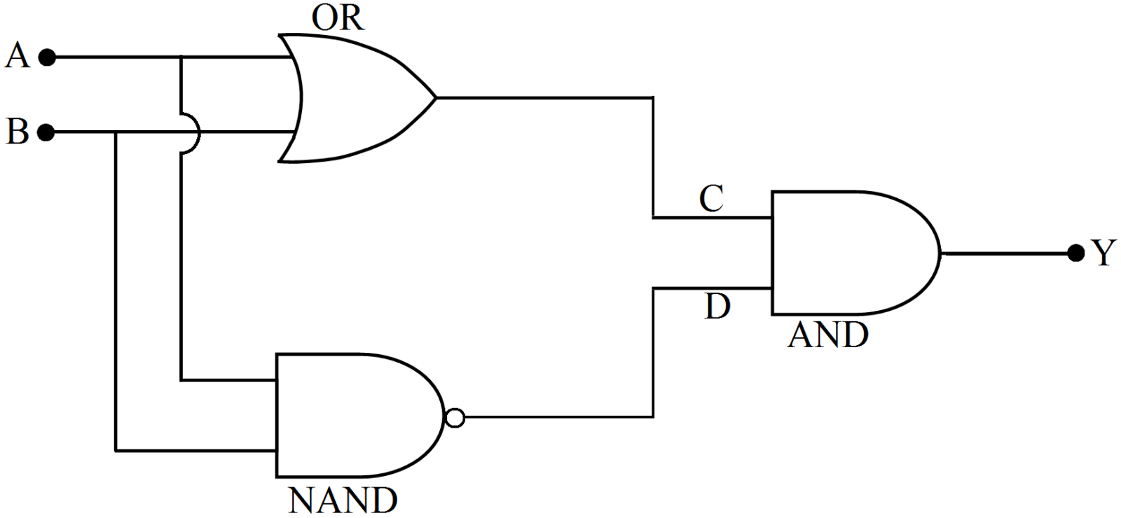
AnswerThe output of OR gate, C = A + B
The output of NAND gate, $\text{D}=\overline{\text{AB}}$
The input of AND gate are C and D, so it's output is $\text{Y}=\text{C}.\text{D}=(\text{A}+\text{B})\overline{\text{AB}}$
When $\text{A}=0,\text{ B}=0,$
$\text{ Y}=(0+0)(0\bar{\cdot}0)=(\text{}0\cdot\bar0)=0\cdot1=0$
When $\text{A}=1,\text{ B}=0,$
$\text{ Y}=(1+0)(1\bar\cdot0)=1\cdot\bar0=1\cdot1=1$
When $\text{A}=0,\text{ B}=1,$
$\text{ Y}=(0+1)(0\bar\cdot1)=1\cdot\bar0=1\cdot1=1$
When $\text{A}=1,\text{ B}=1,$
$\text{ Y}=(1+1)(1\bar\cdot1)=(1\cdot\bar1)=1\cdot0=0$
Thus, truth table of given circuit is:
|
A
|
B
|
Y
|
|
0
|
0
|
0
|
|
1
|
0
|
1
|
|
0
|
1
|
1
|
|
1
|
1
|
0
|
Thia ia the truth table of XOR gate, hence the given circuit represents XOR gate. View full question & answer→Question 783 Marks
There are energy bands in a solid. Do we have really continuous energy variation in a band or do we have very closely spaced but still discrete energy levels?
AnswerA solid consists of a combination of closely spaced energy levels. These energy levels are discrete but they have very small energy gap between two consecutive levels so they are referred as band. However, the energy levels in the band are discrete.
View full question & answer→Question 793 Marks
The output of an OR gate is connected to both the inputs of a NAND gate. Draw the logic circuit of this combination of gates and write its truth table.
AnswerThe logic circuit is shown in fig.
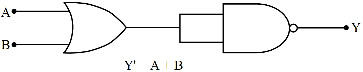
The logic circuit represents NOR gate.
Its truth table is:
|
A
|
B
|
Y'
|
Y
|
|
0
|
0
|
0
|
1
|
|
1
|
0
|
1
|
0
|
|
0
|
1
|
1
|
0
|
|
1
|
1
|
1
|
0
|
View full question & answer→Question 803 Marks
We have valence electrons and conduction electrons in a semiconductor. Do we also have 'valence holes' and 'conduction holes'?
AnswerHoles do not exist in reality. They exist only virtually. When an electron jumps from the valence band to the conduction band, a vacancy is created at the place from where the electron had jumped. This vacancy is called a hole. So, a valence or conduction hole is a virtual concept only.
View full question & answer→Question 813 Marks
Explain the following:
- In the active state of the transistor, the emitter base junction acts as a low resistance while base collection region acts as high resistance.
- Output characteristics are controlled by the input characteristics in common emitter transistor amplifier.
- EDs are made of compound semiconductor and not by elemental semiconductors.
Answer
- Emitter base junction is forward biased whereas collector base junction is reverse biased.
- Small change in the current IB in the base circuit controls the large current IC in the collector circuit $\text{I}_\text{C}=\beta\text{I}_\text{B}.$
- Elemental semiconductor’s band gap is such that the emitted wavelength lies in IR region. Hence cannot be used for making LED.
View full question & answer→Question 823 Marks
Give reasons for the following:
- The Zener diode is fabricated by heavily doping both the p and n sides of the junction.
- A photodiode, when used as a detector of optical signals is operated under reverse bias.
- The band gap of the semiconductor used for fabrication of visible LED’s must at least be 1.8eV.
Answer
- Heavy doping makes the depletion region very thin. This makes the electric field of the junction very high, even for a small reverse bias voltage. This in turn helps the Zener diode to act as a ‘voltage regulator’.
- When operated under reverse bias, the photodiode can detect changes in current with changes in light intensity more easily.
- The photon energy, of visible light photons varies about 1.8eV to 3eV. Hence, for visible LED’s, the semiconductor must have a band gap of 1.8eV.
View full question & answer→Question 833 Marks
Answer the following question:
- Write the truth table of the following gate.
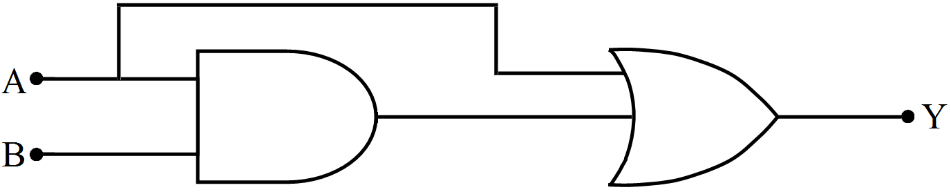
- What will be the values of inputs A and B for the Boolean expression.
$\text{A}\bar{+}\text{B}).(\text{A}\bar{.}\text{B})=1$ AnswerTruth table of the given gate:
| Input |
|
Output |
| A |
B |
Y = A + AB |
| 0 |
0 |
0 |
| 1 |
0 |
1 |
| 0 |
1 |
0 |
| 1 |
1 |
1 |
A = 0, B = 0
Other then $(\text{A}\bar{+}\text{B}).(\overline{\text{AB}})=(0\bar{+}0)(0\bar{.}0)=\bar{0}.\bar{0}=1.1=1$ View full question & answer→Question 843 Marks
(i) Write the name of device 'Y' in the following given diagram
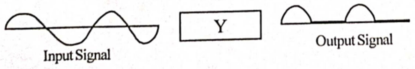
(ii) Draw the circuit diagram of device 'Y'.
(iii) If the frequency of input signal is 60 Hz than what is the frequency of the output signal in a full wave rectifier?
Answer(i) Device 'Y' is a Full Wave Rectifier.
(iii) If input frequency is 60 Hz, output frequency is 120 Hz (Output frequency = $2 \times$ Input frequency).
View full question & answer→Question 853 Marks
(i) Define rectification.
(ii) Draw circuit diagram of a full-wave rectifier.
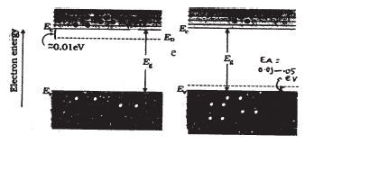
(iii) Semi-conductor related to given energy band diagram is:
n-type semi-conductor, p-type semi-conductor or intrinsic semiconductor.
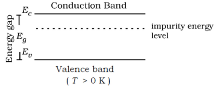
Answer(i) Rectification: Process of converting AC to DC. (iii) The given diagram represents an n-type semiconductor because the impurity energy level is just below the conduction band.
View full question & answer→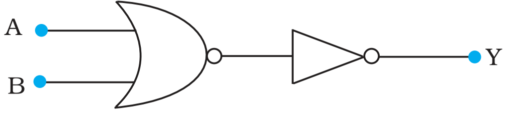


 Alternate Answer
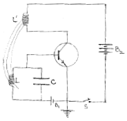 Explanation: By the process of mutual induction (or inductive coupling), energy is fedback to the tank circuit, in phase. The output in an oscillator is selfsustained.