Questions

4 Marks Questions

Take a timed test

12 questions · self-marked practice — reveal the answer and mark yourself.

Question 14 Marks
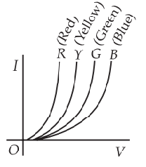
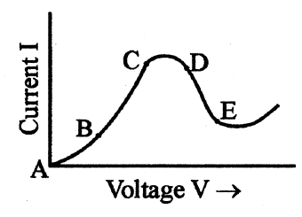
Graph showing the variation of current versus voltage for a material GaAs is shown in the figure. Identify the region of.
  1. Negative resistance.
  2. Where Ohm's law is obeyed.
Answer
DE: Negative resistance region.
AB: Where Ohm's law is obeyed.(Also accept BC).
View full question & answer
Question 24 Marks
  1. State briefly the processes involved in the formation of p-n junction explaining clearly how the depletion region is formed.
  2. Using the necessary circuit diagrams, show how the V-I characteristics of a p-n junction are obtained in
  1. Forward biasing.
  2. Reverse biasing.
How are these characteristics made use of in rectification?
Answer
  1.  

Two processes involved during the formation of p-n junction are diffusion and drift. Due to the concentration gradient, across p and n sides of the junction, holes diffuse from p → n, and electrons from n→ p. This movement of charge carriers leaves behind ionised acceptors on the p-side and donors on the n- side of the junction. This space charge region on either side of the junction, together, is known as depletion region.
  1.  

Using the circuit arrangements shown in fig (a) and fig (b), we study the variation of current with applied voltage to obtain the V-I characteristics shown below.

From the V-I characteristics of a junction diode. it is clear that it allows the current to pass only when it is forward biased. So when an alternatively voltage is applied across the diode, current flows only during that part of the cycle when it is forward biased.
View full question & answer
Question 34 Marks
A silicon $p-n$ junction diode is connected to a resistor Rand a battery of voltage $V_B$ through milliammeter $(mA)$ as shown in figure. The knee voltage for this junction diode is $V_N = 0.7V$. The $p-n$ junction diode requires a minimum current of $1 mA$ to attain a value higher than the knee point on the $I-V$ characteristics of this junction diode. Assuming that the voltage Vacross the junction is independent of the current above the knee point. A $p-n$ junction is the basic building block of many semiconductordevices like diodes. Important process occurring during the formation of a $p-n$ junction are diffusion and drift. ln an $n-$type semiconductor concentration of electrons is more as compared to holes. ln a $p-$ type semiconductor concentration of holes is more as compared to electrons.
  1. If $V_{B }= 5V,$ the maximum value of $R$ so that the voltage $V$ is above the knee point voltage is:
  1. $40\text{k}\Omega$
  2. $4.3\text{k}\Omega$
  3. $5.0\text{k}\Omega$
  4. $5.7\text{k}\Omega$
  1. If $V_B = 5V,$ the value of $R$ in order to establish a current to $6mA$  in the circuit is:
  1. $833\Omega$
  2. $717\Omega$
  3. $950\Omega$
  4. $733\Omega$
  1. If $V_B = 6V,$ the power dissipated in the resistor $R,$ when a current of $6mA$ flows in the circuit is:
  1. $30.2mW$
  2. $30.8mW$
  3. $31.2mW$
  4. $31.8mW$
  1. When the diode is reverse biased with a voltage of $6V$ and $V_{bi} = 0.63V$. Calculate the total potential.
  1. $9.27V$
  2. $6.63V$
  3. $5.27V$
  4. $0.63V$
  1. Which of the below mentioned statement is false regarding a $p-n$ junction diode?
  1. Diodes are uncontrolled devices.
  2. Diodes are rectifying devices.
  3. Diodes are unidirectional devices.
  4. Diodes have three terminals.
Answer
  1. $(b)\ 4.3\text{k}\Omega$
Voltage drop across $R$.
$V_R = V_B - V_N= 5 - 0.7 = 4.3V$
Here $, I_{min} = 1 \times 10^{-3}A$
$\text{R}_\text{max}=\frac{\text{V}_\text{R}}{\text{I}_\text{min}}=\frac{4.3}{1\times10^{-3}}$
$=4.3\times10^3\Omega=4.3\text{k}\Omega.$
  1. $(b)\ 717\Omega$
$I = 6mA = 6 \times 10^{-3}A;$
$V_R = V_B - V_N= 5 - 0.7 = 4.3V$
$\text{R}=\frac{\text{V}_\text{R}}{\text{I}}=\frac{4.3}{6\times10^{-3}}=717\Omega.$
  1. $(d) \ 31.8mW$
Here $, V_{B }= 6V; V_N = 0.7V,$
$V_R = 6 - 0.7 = 5.3V$
Power dissipated in $R =I \times V_R$
$= (6 \times 10^{-3}) \times 5.3 = 31.8 \times 10^{-3}W$
$= 31.8mW$
  1. $(b)\  6.63V$
$V_t = V_{bi} + V_R = 0.63 + 6 = 6.63V.$
  1. $(d)$ Diodes have three terminals.
​​​​​​​Diode is two terminal device, anode and cathode are the two terminals.
View full question & answer
Question 44 Marks
From Bohr's atomic model, we know that the electrons have well defined energy levels in an isolated atom. But due to interatomic interactions in a crystal, the electrons of the outer shells are forced to have energies different from those in isolated atoms. Each energy level splits into a number of energy levels forming a continuous band. The gap between top of valence band and bottom of the conduction band in which no allowed energy levels for electrons can exist is called energy gap.
  1. In an insulator energy band gap is:
  1. $E_{g }= 0$
  2. $E_g < 3eV$
  3. $E_g > 3eV$
  4. None of the above.
  1. In a semiconductor, separation between conduction and valence band is of the order of:
  1. $0eV$
  2. $1eV$
  3. $10eV$
  4. $50eV$
  1. Based on the band theory of conductors, insulators and semiconductors, the forbidden gap is smallest in:
  1. Conductors.
  2. Insulators.
  3. Semiconductors.
  4. All of these.
  1. Carbon, silicon and germanium have four valence electrons each.
  2. At room temperature which one of the following statements is most appropriate?
  1. The number of free electrons for conduction is significant only in $Si$ and $Ge$ but small in $C$.
  2. The number of free conduction electrons is significant in $C$ but small in $Si $ and $Ge$.
  3. The number of free conduction electrons is negligibly small in all the three.
  4. The number of free electrons for conduction is significant in all the three.
  1. Solids having highest energy level partially filled with electrons are:
  1. Semiconductor.
  2. Conductor.
  3. Insulator.
  4. None of these.
Answer
  1. $(c)\ E_g > 3eV$
In insulator, energy band gap is $ > 3eV.$
  1. $(b) \ 1eV$
In conductor, separation between conduction and valence bands is zero and in insulator, it is greater than $1eV.$
Hence in semiconductor the separation between conduction and valence band is $ 1eV.$
  1. $(a)$ Conductors.
According to band theory the forbidden gap in conductors $\text{E}_\text{g}\approx0$ in insulators $E_g > 3eV$ and in semiconductors $E_g < 3eV$.
  1. $(a) $ The number of free electrons for conduction is significant only in $Si$ and $Ge$ but small in $C.$

The four valence electrons of $C, Si,$ and $Ge$ lie respectively in the second, third and fourth orbit. Hence energy required to take out an electron from these atoms $($i.e. ionisation energy $E_g)$ will be least for $Ge,$ followed by $Si,$ and highest for $C$.
Hence, the number of free electrons for conduction in $Ge$ and $Si$ are significant but negligibly small for $C$.
  1. $(b)$ Conductor.
View full question & answer
Question 54 Marks
Light emitting diode is a photoelectric device which converts electrical energy into light energy. It is a heavily doped $p-n$ junction diode which under forward biased emits spontaneous radiation. The general shape of the $I-V$ characteristics of an $\text{LED}$ is similar to that of a normal $p-n$ junction diode, as shown. The barrier potentials are much higher and slightly different for each colour.
  1. The $I-V$ characteristic of an $\text{LED}$ is:
  1. The schematic symbol of light emitting diode is $\text{(LED)}.$
  1. An $\text{LED}$ is constructed from a p-n junction based on a certain $Ga-$ As $-P$ semiconducting material whose energy gap is $1.9eV$. Identify the colour of the emitted light.
  1. Blue.
  2. Red.
  3. Violet.
  4. Green.
  1. Which one of the following statement is not correct in the case of light emitting diodes?
  1. It is a heavily doped $p-n$ junction.
  2. It emits light only when it is forward biased.
  3. It emits light only when it is reverse biased.
  4. The energy of the tight emitted is less than the energy gap of the semiconductor used.
  1. The energy of radiation emitted by $\text{LED}$ is:
  1. Greater than the band gap of the semiconductor used.
  2. Always less than the band gap of the semiconductor used.
  3. Always equal to the band gap of the semiconductor used.
  4. Equal to or less than the band gap of the semiconductor used.
Answer
  1. $(b)$

The $I-V$ characteristics of an $\text{LED}$ is similar to that of a $Si$ junction diode.
But the threshold voltages are much higher and slightly different for each colour.
  1. $(b)$
  1. $(b)$ Red.
As $\text{E}_\text{g}=\frac{\text{hc}}{\lambda}$
$\therefore\lambda=\frac{\text{hc}}{\text{E}_\text{g}}$
Here $, E_{g }= 1.9ev, hc = 1240eVnm$
$\therefore\lambda=\frac{1240\text{eVnm}}{1.9\text{eV}}=652.6\text{ nm}$
Hence, the emitted light is of red colour.
  1. $(c)$ It emits light only when it is reverse biased.
A light emitting diode is a heavily doped $p-n$ junction diode which emits light only when it is forward biased.
  1. $(d)$ Equal to or less than the band gap of the semiconductor used.
View full question & answer
Question 64 Marks
When the diode is forward biased, it is found that beyond forward voltage $V = V_k,$ called knee voltage, the conductivity is very high. At this value of battery biasing for $p-n$ junction, the potential barrier is overcome and the current increases rapidly with increase in forward voltage.
When the diode is reverse biased, the reverse bias voltage produces a very small current about a few microamperes which almost remains constant with bias. This small current is reverse saturation current.
  1. In which of the following figures, the $p-n$ diode is forward biased.
  1.  
  1.  
  1.  
  1.  
  1. Based on the $V-I$ characteristics of the diode, we can classify diode as:
  1. $Bi-$ directional device.
  2. Ohmic device.
  3. Non $-$ ohmic device.
  4. Passive element.
  1. The $V-I$ characteristic of a diode is shown in the figure. The ratio of forward to reverse bi as resistance is:
  1. $100$
  2. $10^6$
  3. $10$
  4. $10^{-6}$
  1. In the case of forward biasing of a $p-n$ junction diode, which one of the following figures correctly depicts the direction of conventional current $($indicated by an arrow mark$)$?
  1.  
  1.  
  1.  
  1.  
  1. If an ideal junction diode is connected as shown, then the value of the current I is:
  1. $0.013A$
  2. $0.02A$
  3. $0.01A$
  4. $0.1A$
Answer
  1. $(c)$

The $p-n$ diode is forward biased when $p-$ side is at a higher potential than $n-$ side.
  1. $(c)$ Non $-$ ohmic device.
  2. $(d) 10^{-6}$
Forward bias resistance,
$\text{R}_1=\frac{\triangle\text{V}}{\triangle\text{I}}=\frac{0.8-0.7}{(20-10)\times10^{-6}}$
$=\frac{0.1}{10\times10^{-3}}=10$
Reverse bias resistance, $\text{R}_2=\frac{10}{1\times10^{-6}}=10^7$
Then, the ratio of forward to reverse bias resistance,
$\frac{\text{R}_1}{\text{R}_2}=\frac{10}{10^7}=10^{-6}$​​​​​​​
  1. $(d) $

In p-region the direction of conventional current is same as flow of holes. In $n-$ region, the direction of conventional current is opposite to the flow of electrons.
  1. $(c)\  0.01A$
In the given circuit the junction diode is forward biased and offers zero resistance.
$\therefore$ The current, $\text{I}=\frac{\text{3V-1V}}{200\Omega}=\frac{\text{2V}}{200\Omega}=0.01\text{A}.$​​​​​​​
View full question & answer
Question 74 Marks

Solar cell is a p-n junction diode which converts solar energy into electric energy. It is basically a solar energy converter. The upperlayer of solar cell is of p-type semiconductor and very thin so that the incident light photons may easily reach the p-n junction. On the top face of p-layer, the metal finger electrodes are prepared in order to have enough spacing between the fingers for the lights to reach the p-n junction through p-layer.
  1. The schematic symbol of solar cell is:
  1. The p-n junction which generates an emf when solar radiations fall an it, with no external bias applied, is a:
  1. Light emitting diode.
  2. Photodiode.
  3. Solar cell.
  4. None of these.
  1. For satellites the source of energy is:
  1. Solar cell.
  2. Fuel cell.
  3. Edison cell.
  4. None of these.
  1. Which of the following material is used in solar cell?
  1. Barium.
  2. Silicon.
  3. Silver.
  4. Selenium.
  1. The efficiency of a solar cell may be in the range:
  1. 2 to 5%
  2. 10 to 15%
  3. 30 to 40%
  4. 70 to 80%
Answer
  1. (a) 
  1. (c) Solar cell.
  2. (a) Solar cell.
Explanation:
Solar cells are the source of energy for satellites.
  1. (b) Silicon.
Explanation:
Silicon is used in solar cell.
  1. (b) 10 to 15%
View full question & answer
Question 84 Marks
A photodiode is an optoelectronic device in which current carriers are generated by photons through photo $-$ excitation i.e., photo conduction by light. It is a $p-n$ junction fabricated from a photosensitive semiconductor and provided with a transparent window so as allow light to fall on its function. A photodiode can turn its current $ON$ and $\text{OFF}$ in nanoseconds. So, it can be used as a fastest photo $-$ detector.
  1. A $p-n$ photodiode is fabricated from a semiconductor with a band gap of $2.5\ eV$. It can detect a signal of wavelength:
  1. $4000\ nm.$
  2. $6000\ nm.$
  3. $4000Â.$
  4. $6000Â.$
  1. Three photo diodes $D_1 ,D_2$ and $D_3$ are made of semiconductors having band gap of $2.5\ eV, 2\ eV,$ and $3 \ eV ,$ respectively. Which one will be able to detect light of wavelength $6000Â$?
  1. $D_1$
  2. $D_2$
  3. $D_3$
  4. $D_1$ and $D_2$ both.
  1. Photodiode is a device:
  1. Which is always operated in reverse bias.
  2. Which of always operated in forward bias.
  3. In which photo current is independent of intensity of incident radiation.
  4. Which may be operated in forward or reverse bias.
  1. To detect light of wavelength $500\ nm,$ the photodiode must be fabricated from a semiconductor of minimum bandwidth of:
  1. $1.24\ eV$
  2. $0.62\ eV$
  3. $2.48\ eV$
  4. $3.2eV$
  1. Photodiode can be used as a photodetector to detect :
  1. Optical signals.
  2. Electrical signals.
  3. Both $(a)$ and $(b)$.
  4. None of these.
Answer
  1. $(c)\ 4000Â.$
$\lambda_\text{max}=\frac{\text{hc}}{\text{E}}=\frac{6.6\times10^{-34}\times3\times10^8}{2.5\times1.6\times10^{-19}}$
$= 5000Â$
$\therefore\lambda=4000\widehat{\text{A}}<\lambda_\text{max}$
  1. $(b)\ D_2$
Energy of incident photon $,\text{E}=\frac{\text{hc}}{\lambda}$
$=\frac{6.6\times10^{-34}\times3\times10^8}{6\times10^{-7}\times1.6\times10^{-19}}=2.06\text{eV}$
The incident radiation can be detected by a photodiode if energy of incident photon is greater than the band gap.
As $D_2 = 2eV,$ therefore $D_2$ will detect these radiations.
  1. $(a)$ Which is always operated in reverse bias.
Photodiode is a device which is always operated in reverse bias.
  1. $(c)\  2.48\ eV$
Let $E_g$ be the required bandwidth. Then
$\text{E}_\text{g}=\frac{\text{hc}}{\lambda}$
Here, he $= 1240eV \ nm,$
$\lambda=500\text{ nm}$
$\therefore\text{E}_\text{g}=\frac{1240\text{eVnm}}{500\text{nm}}=2.48\text{eV}.$
  1. $(a)$ Optical signals.
A photodiode is a device which is used to detect optical signals.
View full question & answer
Question 94 Marks

Rectifier is a device which is used for converting alternating current or voltage into direct current or voltage. Its working is based on the fact that the resistance of p-n junction becomes low when forward biased and becomes high when reverse biased. A half-wave rectifier uses only a single diode while a full wave rectifier uses two diodes as shown in figures (a) and (b).
  1. If the rms value of sinusoidal input to a full wave rectifier is $\frac{\text{V}_0}{\sqrt{2}}$ then the rms value of the rectifier's output is:
  1. $\frac{\text{V}_0}{\sqrt{2}}$
  2. $\frac{\text{V}_0^2}{\sqrt{2}}$
  3. $\frac{\text{V}_0^2}{2}$
  4. $\sqrt{2}\text{V}_0^2$
  1. In the diagram, the input ac is across the terminals A and C. The output across B and D is:
  1. Same as the input.
  2. Half wave rectified.
  3. Zero.
  4. Full wave rectified.
  1. A bridge rectifier is shown in figure. Alternating input is given across A and C. If output is taken across BD, then it is:
  1. Zero.
  2. Same as input.
  3. Half wave rectified.
  4. Full wave rectified.
  1. A p-n junction (D) shown in the figure can act as a rectifier. An alternating current source (V) is connected in the circuit. The current (I) in the resistor (R) can be shown by:

  1. With an ac input from 50Hz power line, the ripple frequency is:
  1. 50Hz in the de output of half wave as well as full wave rectifier.
  2. 100Hz in the de output of half wave as well as full wave rectifier.
  3. 50Hz in the de output of half wave and I 00Hz in de output of full wave rectifier.
  4. 100Hz in the de output of half wave and 50Hz in the de output of full wave rectifier.
Answer
  1. (a) $\frac{\text{V}_0}{\sqrt{2}}$
Explanation:
Therms value of the output voltage at the load resistance, $\frac{\text{V}_0}{\sqrt{2}}.$
  1. (d) Full wave rectified.
  2. (a) Zero.
  3. (c)

Explanation:
The given circuit works as a half wave rectifier. In this circuit, we will get current through R when p-n junction is forward biased and no current when p-n junction is reverse biased. Thus the current (I) through resistor (R) will be shown in option (c).
  1. (c) 50Hz in the de output of half wave and I 00 Hz in de output of full wave rectifier.
View full question & answer
Question 104 Marks
P-n junction is a single crystal of Ge or Si doped in such a manner that one half portion of it acts asp-type semiconductor and other half functions as n-type semiconductor. As soon as a p-n junction is formed, the holes from the p-region diffuse into then-region, and electron from n region diffuse in top-region. This results in the development of V 8 across the junction which opposes the further diffusion of electrons and holes through the junction.
  1. In an unbiased p-n junction electrons diffuse from n-region top-region because:
  1. Holes in p-region attract them.
  2. Electrons travel across the junction due to potential difference.
  3. Electron concentration inn-region is more as compared to that in p-region.
  4. Only electrons move from n top region and not the vice-versa.
  1. Electron hole recombination in p-n junction may lead to emission of:
  1. Light.
  2. Ultraviolet rays.
  3. Sound.
  4. Radioactive rays.
  1. In an unbiased p-n junction:
  1. Potential at pis equal to that at n.
  2. Potential at pis + ve and that at n is - ve.
  3. Potential at pis more than that at n.
  4. Potential at pis less than that at n.
  1. The potential of depletion layer is due to:
  1. Electrons.
  2. Holes.
  3. Ions.
  4. Forbidden band.
  1. In the depletion layer of unbiased p-n junction,
  1. It is devoid of charge carriers.
  2. Has only electrons.
  3. Has only holes.
  4. P-n junction has a weak electric field.
Answer
  1. (c) Electron concentration inn-region is more as compared to that in p-region.
Explanation:
Electron concentration in n-region is more as compared to that in p-region. So electrons diffuse from n-side to p-side.
  1. (a) Light.
​​​​​​​Explanation:
When an electron and a hole recombine, the energy is released in the form of light.
  1. (a) Potential at pis equal to that at n.
​​​​​​​​​​​​​​​​​​​​​Explanation:
In an unbiased p-n junction, potential at p is equal to that at n.
  1. (c) Ions.
​​​​​​​​​​​​​​​​​​​​​​​​​​​​Explanation:
The potential of depletion layer is due to ions.
  1. (a) It is devoid of charge carriers.
​​​​​​​​​​​​​​​​​​​​​​​​​​​​​​​​​​​Explanation:
In the depletion layer of unbiased p-n, junction has no charge carriers.
View full question & answer
Question 114 Marks
The electron mobility characterises how quickly an electron can move through a metal of semiconductor when pulled by an electric field. There is an analogous quality for holes, called hole mobility. A block of pure silicon at $300K$ has a length of $10\ cm$ and an area of $1.0\ cm^2$. A battery of emf $2V$ is connected across it. The mobility of electron is $0.14m^2 V^{-1}s^{-1}$ and their number density is $1.5 \times 10^{16}m^{-3}$. The mobility of holes is $0.05m^2 V^{-1}s^{-1}.$
  1. The electron current is:
  1. $6.72 \times 10^{-4}A$
  2. $6.72 \times 10^{-5}A$
  3. $6.72 \times 10^{-6}A$
  4. $6.72 \times 10^{-7}A$
  1. The hole current is:
  1. $2.0 \times 10^{-7}A$
  2. $2.2 \times 10^{-7}A$
  3. $2.4 \times 10^{-7}A$
  4. $2.6 \times 10^{-7}A$
  1. The number density of donor atoms which are to be added up to pure silicon semiconductor to produce an $n-$ type semiconductor of conductivity $6.4\Omega^{-1}\text{cm}^{-1}$ is approximately $($neglect the contribution of holes to conductivity$)$.
  1. $3 \times 10^{22}m^{-3}$
  2. $3 \times 10^{23}m^{-3}$
  3. $3 \times 10^{24}m^{-3}$
  4. $3 \times 10^{21}m^{-3}$
  1. When the given silicon semiconductor is doped with indium, the hole concentration increases to $4.5 \times 10^{23}m^{-3}$. The electron concentration in doped silicon is:
  1. $3 \times 10^9m^{-3}$
  2. $4 \times 10^9m^{-3}$
  3. $5 \times 10^9m^{-3}$
  4. $6 \times 10^9m^{-3}$
  1. Pick out the statement which is not correct.
  1. At a low temperature, the resistance of a semiconductor is very high.
  2. Movement of holes is restricted to the valence band only.
  3. Width of the depletion region increases as the forward bias voltage increases in case of a $p-n$ junction diode.
  4. ln a forward bias condition, the diode heavily conducts.
Answer
  1. $(d)\  6.72 \times 10^{-7}A$
$\text{E}=\frac{\text{V}}{\text{l}}=\frac{2}{0.1}20\text{V/ m;}$
$A = 1.0\ cm^2 = 1.0 \times 10^{-4}m^2$
$\text{v}_\text{e}=\mu_\text{e}\text{E}=0.14\times20=2.8\text{ms}^{-1}$
$I_e = n_eAev_e$
$= ( 1.5 \times 10^{16}) \times ( 1.0 \times 10^{-4}) \times ( 1.6 \times 10^{-19}) \times 2.8$
$= 6.72 \times 10^{-7}A$
  1. $(c) \ 2.4 \times 10^{-7}A$
In a pure semiconductor,
$n_e = n_h = 1.5 \times 10^{16}m^{-3}$
$\text{v}_\text{h}=\mu_\text{h}\times\text{E}=0.05\times20=1.0\text{ms}^{-1}$
$I_h = n_hAev_h$
$= ( 1.5 \times 10^{16}) \times ( 1.0 \times 10^{-4}) \times ( 1.6 \times 10^{-19}) \times 1.0$
$= 2.4 \times 10^{-7}A$
  1. $(a) \ 3 \times 10^{22}m^{-3}$
$\sigma=\text{en}_\text{e}\text{m}_\text{e}$
Or $\text{n}_\text{e}=\frac{\sigma}{\text{e}\mu_\text{e}}=\frac{6.4\times10^2}{(1.6\times10^{-19}\times0.14}$
$=3.14\times10^{22}\approx3\times10^{22}\text{m}^{-3}$
  1. $(c)\ 5 \times 10^9m^{-3}$
$​​\text{n}_\text{e}=\frac{\text{n}^2_\text{i}}{\text{n}_\text{h}}=\frac{(1.5\times10^{16})^2}{4.5\times10^{22}}$
$= 5 \times 10^9m^{-3}$
  1. $(c)$ Width of the depletion region increases as the forward bias voltage increases in case of a $p-n $ junction diode.
In case of a $p-n$ junction diode, width of the depletion region decreases as the forward bias voltage increases.
View full question & answer
Question 124 Marks
The potential barrier in the $p-n$ junction diode is the barrier in which the charge recquires additional force for crossing the region. ln other words, the barrier in which the charge carrier stopped by the obstructive force is known as the potential barrier.
When a $p-$type semiconductor is brought into a close contact with $n-$ ype semiconductor, we get a $p-n$ junction with a barrier potential $0.4V,$ and width of depletion region is $4.0 \times 10^{-7}m.$ This $p-n$ junction is forward biased with a battery of voltage $3V$ and negligible internal resistance, in series with a resistor of resistance $R,$ ideal millimeter, and key $K$ as shown in figure. When key is pressed, a current of $20\ mA$ passes through the diode.
  1. The intersity of the electric field in the depletion region when $p-n$ junction is unbiased is:
  1. $0.5 \times 10^6\ Vm^{-1}$
  2. $1.0 \times 10^6\ Vm^{-1}$
  3. $2.0 \times 10^6\ Vm^{-1}$
  4. $1.5 \times 10^6\ Vm^{-1}$
  1. The resistance of resistor $R$ is:
  1. $150\Omega$
  2. $300\Omega$
  3. $130\Omega$
  4. $180\Omega$
  1. In a $p-n$ junction, the potential barrier is due to the charges on either side of the junction, these charges are:
  1. Majority carriers.
  2. Minority carriers.
  3. Both $(a)$ and $(b)$.
  4. Fixed donor and acceptor ions.
  1. If the voltage of the potential barrier is $V_0.$ A voltage Vis applied to the input, at what moment will the barrier disappear?
  1. $V < V_0$
  2. $V = V_0$
  3. $V > V_0$
  4. $V << V_0$
  1. If an electron with speed $4.0 \times 10^5ms^{-1}$ approaches the $p-n$ junction from then$-$side, the speed with which it will enter the $p-$side is:
  1. $1.39 \times 10^5\ ms^{-1}$
  2. $2.78 \times 10^5\ ms^{-1}$
  3. $1.39 \times 10^6\ ms^{-1}$
  4. $2.78 \times 10^6\ ms^{-1}$
Answer
  1. $(b) 1.0 \times 10^6\ Vm^{-1}$
$\text{E}-\frac{\text{V}_\text{B}}{\text{d}}=\frac{0.4}{4.0\times10^{-7}}$
$= 1.0 \times 10^6\ Vm^{-1}$
  1. $(c)\ 130\Omega$
Potential difference across $= R = 3 - 0.4 = 2.6V$
Resistance $\text{R}=\frac{\text{Potential difference}}{\text{Current }}$
$=\frac{2.6}{20\times10^{-3}}=130\Omega$
  1. $(d)$ Fixed donor and acceptor ions.
  2. $(b)\ V = V_0$
When the voltage will be the same that of the potential barrier disappears resulting in flow of current.
  1. $(a)\ 1.39 \times 10^5\ ms^{-1}$
$\frac{1}{2}\text{mv}^2_1=\text{eV}_\text{B}+\frac{1}{2}\text{mv}^2_2$
$\Rightarrow\frac{1}{2}\times(9.1\times10^{-31})\times(4\times10^5)^2$
$=1.6\times10^{-19}\times(0.4)+\frac{1}{2}\times9.1\times10^{-31}\times\text{v}^2_2$
On solving, we get
$v_2 = 1.39 \times 10^5\ ms^{-1}$
View full question & answer