Questions · Page 1 of 5

M.C.Q (1 Marks)

🎯

Test yourself on this topic

50 questions · timed · auto-graded

MCQ 11 Mark
The thickness of the depletion region is of the order of $........$ of a micrometre.
  • A
    One$-$hundredth
  • B
    One$-$tenth
  • C
    One$-$thousandth
  • None of these
Answer
Correct option: D.
None of these

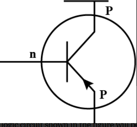
Depletion region is a region near the $p-n$ junction where flow of charge carriers $($free electrons and holes$)$ is reduced over a given period and finally results in zero charge carriers.The width of depletion region which is generally $1\mu m$, depends on the amount of impurities added to the semiconductor. Impurities are the atoms $($pentavalent and trivalent atoms$)$ added to the semiconductor to improve its conductivity.
hence answer is $1\mu$ m and correct option is $D -$ none of these.

View full question & answer
MCQ 21 Mark
In a $p-$type semiconductor, the acceptor valence band is:
  • Close to the valence band of the host crystal.
  • B
    Close to conduction band of the host crystal.
  • C
    Below the conduction band of the host crystal.
  • D
    Above the conduction band of the host crystal.
Answer
Correct option: A.
Close to the valence band of the host crystal.
View full question & answer
MCQ 31 Mark
The energy gap in glass at room temperature is:
  • A
    Greater than that in a semiconductor.
  • B
    Less than that in a good conductor.
  • C
    Greater than that in a good conductor.
  • Both $(1)$ and $(3)$ are true.
Answer
Correct option: D.
Both $(1)$ and $(3)$ are true.

Glass is an insulator. The energy gap in a glass is greater than that of semiconductor and a good conductor.

View full question & answer
MCQ 41 Mark
Two identical capacitors $A$ and $B$ are charged to the same potential $V$ and are connected in two circuits at $t = 0$ as shown in figure. The charges on the capahltors at a time $t = CR$ are, respectively:
  • A
    $\text{VC}, \text{VC}$
  • $\frac{\text{VC}}{\text{e}}, \text{VC}$
  • C
    $\text{VC}, \frac{\text{VC}}{\text{e}}$
  • D
    $\frac{\text{VC}}{\text{e}}, \frac{\text{VC}}{\text{e}}$
Answer
Correct option: B.
$\frac{\text{VC}}{\text{e}}, \text{VC}$

In circuit $(a)$, the diode is forward biassed. So, it offers negligible resistance to the flow of current and can thus be replaced by a short circuit. Now, the capacitor charge will leak through the resistance and decay exponentially with time.
Capacitor charge $=\frac{\text{VC}}{\text{e}}$
In circuit $(b),$ the diode is reverse biassed. So, it offers infinite resistance to the current flow and can thus be replaced by an open circuit. As the circuit is open now, no current can flow across the resistance. So, the charge in the capacitor cannot leak through the resistor.
Capacitor charge $= VC$

View full question & answer
MCQ 51 Mark
There is a sudden increase in current in zener diode is:
  • Due to rupture of bonds
  • B
    Resistance of deplection layer becomes less
  • C
    Due to high doping
  • D
    Due to less doping
Answer
Correct option: A.
Due to rupture of bonds
When Zener diode is connected in reverse bias, as applied voltage reaches at Zener breakdown voltage, due to rupture of bonds there is a sudden increase in current in Zener diode.
View full question & answer
MCQ 61 Mark
The free electron density is more in $.....:$
  • Conductors
  • B
    Insulators
  • C
    Semi conductors
  • D
    Electrolytes
Answer
Correct option: A.
Conductors

Free electron density is more in conductors that is why they are useful in conducting electricity.

View full question & answer
MCQ 71 Mark
The truth table given in figure represents:
$A$ $B$ $Y$
$0$ $0$ $0$
$0$ $1$ $1$
$1$ $0$ $1$
$1$ $1$ $1$
  • A
    $\text{AND} -$ Gate
  • B
    $\text{NOR} -$ Gate
  • C
    $\text{NAND} -$ Gate
  • $\text{OR} -$ Gate
Answer
Correct option: D.
$\text{OR} -$ Gate

$\text{OR}$ gate has the property that output is one when any one of the inputs is one and zero only when all inputs are zero. From the truth table, it can be seen that the above two properties are satisfied.

View full question & answer
MCQ 81 Mark
The value indicated by Fermi energy level in an intrinsic semiconductor is:
  • The average energy of electrons and holes.
  • B
    The energy of electrons in conduction band.
  • C
    The energy of holes in valence band.
  • D
    The energy of forbidden region.
Answer
Correct option: A.
The average energy of electrons and holes.
In an intrinsic semiconductor, $n=p$, where, n is number of electrons and $p$ is number of holes in intrinsic semiconductor.
This implies that there is an equal chance of finding an electron at the conduction band edge as there is of finding a hole at the valence band edge. Thus, the average energy level of electrons and holes is half of the energy band gap in intrinsic semiconductors.
Also the Fermi energy level lie exactly in the middle of energy band gap in intrinsic semiconductors. Thus, the value indicated by Fermi energy level in an intrinsic semiconductor is the average energy of electrons and holes.
View full question & answer
MCQ 91 Mark
In a transistor:
  • A
    The emitter has the least concentration of impurity.
  • B
    The collector has the least concentration of impurity.
  • The base has the least concentration of impurity.
  • D
    All the three regions have equal concentrations of impurity.
Answer
Correct option: C.
The base has the least concentration of impurity.
View full question & answer
MCQ 101 Mark
For the given combination of gates, if the logic states of inputs $\text{A, B, C}$ are as follows $A = B = C = 0$ and $A = B = 1,C = 0$ then the logic states of output $D$ are:
  • $0,0$
  • B
    $0,1$
  • C
    $1, 0$
  • D
    $1,1$
Answer
Correct option: A.
$0,0$
$OR$ gate add the input signals given to it and $\text{AND}$ gate multiply the input signals given to it.
Input $(0,0)$ given to $OR$ gate will yield result $0.$
Now input for $\text{AND}$ gate are $(0,0)$ hence output will be $0.$
For the second case, input $(1,1)$ given to $OR$ gate will yield result $1.$
Now input for $\text{AND}$ gate are $(1,0)$ hence output will be $0.$
Therefore combination of gates will yield result $0$ and $0.$
View full question & answer
MCQ 111 Mark
When an electric field is applied across a semiconductor:
  • A
    Electrons move from lower energy level to higher energy level in the conduction band.
  • B
    Electrons move from higher energy level to lower energy level in the conduction band.
  • C
    Holes in the valence band move from higher energy level to lower energy level.
  • A and C both
Answer
Correct option: D.
A and C both
Solution:
As we apply electric field is applied across a semiconductor, the electrons in the conduction band acquire energy and get accelerated. They travel from lower energy level to higher energy level. While the holes in valence band travel from higher energy level to lower energy level, where they will be having more energy.
View full question & answer
MCQ 121 Mark
Generally semiconductor can be used safely between the temperatures:
  • A
    $−75$ and $200$
  • $0$ and $75$
  • C
    $−25$ and $300$
  • D
    $−40$ and $1000$
Answer
Correct option: B.
$0$ and $75$
Semiconductor can be used safely between temperature $0$ and $75.$
View full question & answer
MCQ 131 Mark
Carbon, silicon and germanium have four valence electrons each. At room temperature the appropriate statement is:
  • A
    The number of free electrons for conduction is significant only in Si and Ge but small in $C.$
  • B
    The number of free conduction electrons is significant in $C$ but small $Si$ and Ge.
  • The number of free conduction electrons is negligibly small in all the three.
  • D
    The number of free conduction electrons is significant in all the three.
Answer
Correct option: C.
The number of free conduction electrons is negligibly small in all the three.

In Si and Ge at room temperature $(300K);$ the energy band gap is low as the result of which electrons in the covalent bonds gain kinetic energy, they break the bond and move to conduction band.
A hole is also created in the valence band. So the number of free electrons for conduction is significant in $Si$ and Ge.
The energy band gap in case of carbon is high as the result of which there are not significant number of electrons in the conduction band even at room temperature.

View full question & answer
MCQ 141 Mark
The gate for which output is high if atleast one input is low?
  • A
    $\text{NAND.}$
  • B
    $\text{NOR.}$
  • C
    $\text{AND.}$
  • $\text{OR.}$
Answer
Correct option: D.
$\text{OR.}$
View full question & answer
MCQ 151 Mark
A semiconductor is doped with a donor impurity:
  • A
    The hole concentration increases.
  • B
    The hole concentration decreases.
  • The electron concentration increases.
  • D
    The electron concentration decreases.
Answer
Correct option: C.
The electron concentration increases.

When a semiconductor is doped with a donor type such as arsenic or phosphorous, which has five valence electrons, the donor atom replaces the $Si$ or $Ge$ atom. As a result, four out of the five electrons of the donor atom form a covalent bond by sharing an electron with four atoms of silicon. However, the fifth electron is free to move. Also, due to the breaking up of covalent bonds at room temperature, equal number of electrons and holes are produced. Thus, the total number of holes in the $n-$type semiconductor is less compared to the number of free electrons.

View full question & answer
MCQ 161 Mark
The lead marked with the arrow is the $........$
  • A
    collector
  • B
    base
  • emitter
  • D
    core
Answer
Correct option: C.
emitter

It is a $p-n-p,$ transistor. The Lead marked with the arrow is the emitter. It tells the direction of the flow of the holes i.e, the flow of conventional current.

View full question & answer
MCQ 171 Mark
The following truth table is for: $\text{ABY 110 101 011 001}$
  • $\text{NAND}$ gate
  • B
    $\text{AND}$ gate
  • C
    $\text{XOR}$ gate
  • D
    $\text{NOT}$ gate
Answer
Correct option: A.
$\text{NAND}$ gate

The output is $0$ only when the two inputs are $1.$
The output is $1$ when any of the input is zero.
This is the characteristic of a $\text{NAND}$ gate.

View full question & answer
MCQ 181 Mark
The energy gap between the valence band and the condition band for a material is $6\ eV$. The material is?
  • An insulator
  • B
    A metal
  • C
    An intrinsic semiconductor
  • D
    A superconductor
Answer
Correct option: A.
An insulator
Insulators have large energy gap between valence and conduction band $($about $6\ eV)$, while semiconductors have a smaller one and conductors, the smallest energy gap.
View full question & answer
MCQ 191 Mark
In an intrinsic semiconductor, the number of electrons in the conduction band is $........$ the number of holes in the valence band.
  • Equal to
  • B
    Less than
  • C
    Greater than
  • D
    None of these
Answer
Correct option: A.
Equal to

In an intrinsic semiconductor, the number density of electrons is equal to the number density of holes i.e ne $=$ nh.
Since there is no doping, no extra hole or electron is produced.

View full question & answer
MCQ 201 Mark
Filter circuit:
  • Eliminates $a.c.$ component.
  • B
    Eliminates $d.c.$ component.
  • C
    Does not eliminate $a.c.$ component.
  • D
    None of these.
Answer
Correct option: A.
Eliminates $a.c.$ component.
View full question & answer
MCQ 211 Mark
By increasing the temperature, the specific resistance of a conductor and a semiconductor:
  • A
    Increases for both.
  • B
    Decreases for both.
  • Increases, decreases.
  • D
    Decreases, increases.
Answer
Correct option: C.
Increases, decreases.
View full question & answer
MCQ 221 Mark
The main cause of avalanche breakdown is:
  • Ionisation by collision.
  • B
    High doping.
  • C
    Recombination of electrons and holes.
  • D
    Low doping.
Answer
Correct option: A.
Ionisation by collision.

Avalanche breakdown is caused by impact ionization of electron-hole pairs. A very little current flows under reverse bias conditions and depletion region increases. The electric field in the depletion region of a diode can be very high. Electron/holes that enter the depletion region undergo a tremendous acceleration.
As these accelerated carriers collide with the atoms, they can knock electrons from their bonds, creating additional electron/hole pairs and thus additional current. As these secondary carriers are swept into the depletion region, they too are accelerated and the process repeats itself.

View full question & answer
MCQ 231 Mark
At absolute zero, $Si$ acts as:
  • A
    Non$-$metal.
  • B
    Metal.
  • Insulator.
  • D
    None of these.
Answer
Correct option: C.
Insulator.
View full question & answer
MCQ 241 Mark
When an input signal $1$ is applied to a $\text{NOT}$ gate, its output is:
  • A
    $1$
  • $0$
  • C
    either $0$ or $1$
  • D
    both $0$ and $1$
Answer
Correct option: B.
$0$

$\text{NOT}$ gate yields the reverse of the input signal in output, thus when an input signal $1$ is applied to a $\text{NOT}$ gate, its output is $0.$

View full question & answer
MCQ 251 Mark
The gate that has only one input terminal:
  • $\text{NOT}$
  • B
    $\text{NOR}$
  • C
    $\text{NAN}$
  • D
    $\text{XOR}$
Answer
Correct option: A.
$\text{NOT}$

Only one logic gate has one input terminal i.e. $\text{NOT}$ gate.

View full question & answer
MCQ 261 Mark
When a $P - N$ junction is unbiased, the junction current at equilibrium is:
  • Zero as no charges cross the junctions.
  • B
    Zero as equal number of charge carriers cross the barrier in opposite directions.
  • C
    Mainly due to diffusion of majority charge carriers.
  • D
    Mainly due to diffusion of minority charge carriers.
Answer
Correct option: A.
Zero as no charges cross the junctions.

When a diode is connected in a Zero Bias condition, no external potential energy is applied to the $PN$ junction. However if the diodes terminals are shorted together, a few holes $($majority carriers$)$ in the $P-$type material with enough energy to overcome the potential barrier will move across the junction against this barrier potential. This is known as the Forward Current.
Likewise, holes generated in the $N-$type material $($minority carriers$)$, find this situation favourable and move across the junction in the opposite direction. This is known as the Reverse Current and is referenced as $IR$. This transfer of electrons and holes back and forth across the $PN$ junction is known as diffusion.
Then an Equilibrium or balance will be established when the majority carriers are equal and both moving in opposite directions so that the net result is zero current flowing in the circuit. When this occurs the junction is said to be in a state of Dynamic Equilibrium.

View full question & answer
MCQ 271 Mark
The conductivity of a semiconductor increases with increase in temperature because:
  • A
    Number density of free current carriers increases.
  • B
    Relaxation time increases.
  • C
    Both number density of carriers and relaxation time increase.
  • Number density of current carriers increases, relaxation time decreases but effect of decrease in relaxation time is much less than increase in number density.
Answer
Correct option: D.
Number density of current carriers increases, relaxation time decreases but effect of decrease in relaxation time is much less than increase in number density.

With increase in temperature, the number density of current carries increases, relaxation time decreases but effect of decrease in relaxation is much less than increase in number density. So, the conductivity of a semiconductor increases with increase in temperature.

View full question & answer
MCQ 281 Mark
In Boolean algebra, $A + B = Y$ implies that:
  • A
    sum of $A$ and $B$ is $Y.$
  • $Y$ exists when $A$ exists or $B$ exists or both $A$ and $B$ exist.
  • C
    $Y$ exists only when $A$ and $B$ both exist.
  • D
    $Y$ exists when $A$ or $B$ exist but not when both $A$ and $B$ exist.
Answer
Correct option: B.
$Y$ exists when $A$ exists or $B$ exists or both $A$ and $B$ exist.

In Boolean algebra, $A + B = Y$ implies that $Y$ exists when $A$ exists or $B$ exists or both $A$ and $B$ exist.

View full question & answer
MCQ 291 Mark
A $p-$type semiconductor is:
  • A
    Positively charged.
  • B
    Negatively charged.
  • Uncharged.
  • D
    Uncharged at $0K$ but charged at higher temperatures.
Answer
Correct option: C.
Uncharged.
View full question & answer
MCQ 301 Mark
At breakdown voltage, the rate of creation of hole-electron pairs is $........$ leading to the $........$ in current.
  • A
    increased, decrease
  • increased, increase
  • C
    decreased, increase
  • D
    decreased, decrease
Answer
Correct option: B.
increased, increase

When the reverse voltage across a diode is very large, the valance electrons become free due to applied high electric field and get enough acceleration to make other electrons free, thus create a lot of electron-hole pairs in a short time. As the number of charge carriers increases, current also increases.
Therefore, at breakdown voltage, the rate of creation of hole$-$electron pairs is increased leading to the increase in current.

View full question & answer
MCQ 311 Mark
In semiconductors, at a room temperature:
  • The valence band is partially empty and the conduction band is partially filled.
  • B
    The valence band is completely filled and the conduction band is partially filled.
  • C
    The valence band is completely filled.
  • D
    The conduction band is completely empty.
Answer
Correct option: A.
The valence band is partially empty and the conduction band is partially filled.

In semiconductors at room temperature the electrons get enough energy so that they are able to over come the forbidden gap. Thus at room temperature the valence band is partially empty and conduction band is partially filled.

View full question & answer
MCQ 321 Mark
In the given circuit, if $A$ and $B$ represent two inputs and $C$ represents the output, the circuit represents:
  • A
    $\text{NOR}$ gate
  • B
    $\text{AND}$ gate
  • C
    Gate
  • $\text{OR}$ gate
Answer
Correct option: D.
$\text{OR}$ gate

The image given shows a diode $\text{OR}$ circuit. $R$ is connected from the output to ground to provide bias current for the diodes. Any positive voltage will represent a logic $1$ state and the summing of currents through multiple diodes does not change the logic level.

View full question & answer
MCQ 331 Mark
In an experiment of photoelectric effect the number of photoelectrons has to be increased without changing their frequency. The suitable step to be taken about the incident radiation for this is:
  • Increasing intensity without changing frequency.
  • B
    Increase both frequency and intensity.
  • C
    Increase frequency without increasing intensity.
  • D
    Increasing only frequency
Answer
Correct option: A.
Increasing intensity without changing frequency.

Intensity of photons is the number of photons passing through a cross sectional area per unit time. Hence changing the intensity would cause change in number of ejected photoelectrons emitted by them.

View full question & answer
MCQ 341 Mark
In a semiconductor, which of the following statement is correct?
  • A
    At $0K$, Si is a super conductor.
  • B
    In a $p-$type semiconductor the acceptor level lies near the conduction band.
  • C
    Each donor atom contributes one hole.
  • $p - n$ junction is electrically neutral.
Answer
Correct option: D.
$p - n$ junction is electrically neutral.

Generally $Si$ is a semiconductor. In $p$ type semiconductor acceptor level lies near the valence band and each donor atom contribute one electron. $p-n$ junction electrically neutral because total charge is zero.

View full question & answer
MCQ 351 Mark
The impurity atoms with which pure silicon may be doped to make it a p-type semiconductor are those of:
  • A
    Phosphorus.
  • B
    Boron.
  • C
    Aluminium.
  • B and C both
Answer
Correct option: D.
B and C both
Explanation:
A p-type semiconductor is formed by doping an intrinsic semiconductor with a trivalent atom (atom having valency 3). As phosphorous and boron have three valence electrons, they can be doped with silicon to make a p-type semiconductor.
View full question & answer
MCQ 361 Mark
Materials which allow only larger currents to flow through them are:
  • A
    Insulators
  • Semi$-$conductors
  • C
    Conductors
  • D
    Alloys
Answer
Correct option: B.
Semi$-$conductors

Semiconductors in their natural state are poor conductors because a current requires the flow of electrons, and semiconductors have their valence band filled, preventing the entry flow of new electrons.
Thus semi$-$conductors allows a large current to pass through them.

View full question & answer
MCQ 371 Mark
Two important processes that occur during the formation of a $p-n$ junction.
  • A
    Diffusion
  • B
    Drift
  • Both drift and diffusion
  • D
    Drift in $p$ region and diffusion in $n$ region
Answer
Correct option: C.
Both drift and diffusion

Three important phenomena occurs during formation of pn junction:
Diffusion, Formation of space charge, Drift.

View full question & answer
MCQ 381 Mark
The avalanche breakdown in $p-n$ junction is due to:
  • A
    Shift of Fermi level.
  • Cumulative effect of conduction band electron.
  • C
    Widening of forbidden gap.
  • D
    High impurity concentration.
Answer
Correct option: B.
Cumulative effect of conduction band electron.

The avalanche breakdown in $p-n$ junction is due to cumulative effect of conduction band electron. In reverse bias, due to applied electric field, electrons acquire enough energy to free more electron bound to the atom. The abundant number of electron$-$hole pairs are created for conduction, this is cumulative effect.

View full question & answer
MCQ 391 Mark
Among the following one can act as the building blocks for the other gates is:
  • $\text{NAND}$ and $\text{NOR}$
  • B
    $\text{NAND}$ and $\text{AND}$
  • C
    $\text{XOR}$ and $\text{OR}$
  • D
    $\text{NOT}$ and $\text{OR}$
Answer
Correct option: A.
$\text{NAND}$ and $\text{NOR}$

$\text{NAND}$ and $\text{NOR}$ gates are known as universal gates. Any one of these gates can be used to implement any kind of logic gate. This kind of feasibility is does not exist with other gates i.e. any other gate cannot solely implement all logic gates. For example, $\text{AND}$ gate cannot be implemented using an $\text{OR}$ gate and vice$-$versa. The implementation of $\text{NAND}$ and $\text{NOR}$ gates to generate other logic gates is shown above.

View full question & answer
MCQ 401 Mark
Hole in semiconductor is:
  • A
    An anti $–$ particle of electron.
  • B
    A vacancy created when an electron leaves a covalent bond.
  • C
    Absence of free electrons.
  • An artificially created particle.
Answer
Correct option: D.
An artificially created particle.
View full question & answer
MCQ 411 Mark
In an insulator, the forbidden energy gap between the valence band and conduction band is of the order of:
  • A
    $1\ MeV.$
  • B
    $0.1\ MeV.$
  • C
    $1\ eV.$
  • $5\ eV.$
Answer
Correct option: D.
$5\ eV.$
View full question & answer
MCQ 421 Mark
If the two ends of a $p-n$ junction are joined by a wire:
  • There will not be a steady current in the circuit.
  • B
    There will be a steady current from the $n-$side to the pside.
  • C
    There will be a steady current from the $p-$side to the nside.
  • D
    There may or may not be a current depending upon the resistance of the connecting wire.
Answer
Correct option: A.
There will not be a steady current in the circuit.
View full question & answer
MCQ 431 Mark
The diffusion current in a $p-n$ junction is:
  • A
    From the n-side to the $p-$side.
  • From the $p-$side to the $n-$side.
  • C
    From the $n-$side to the p-side if the junction is forward$-$biased and in the opposite direction if it is reverse$-$biased.
  • D
    From the $p-$side to the $n-$side if the junction is forward$-$biased and in the opposite direction if it is reverse$-$biased.
Answer
Correct option: B.
From the $p-$side to the $n-$side.

When a $p‒n$ junction is formed then because of the difference in the concentration of charge carriers in the two regions, electrons from the $n$ region move to the $p$ region and holes from the $p$ region move to the $n$ region. Since the direction of the current is always opposite to the motion of electron, the direction of the current is from the $p$ side to the n side.
Similarly, when the junction is forward biassed, the positive terminal of the battery is connected to the pside of the $p‒n$ junction and the negative terminal of the battery is connected to the n side of the $p‒n$junction. As a result, electrons in the n side of the $p‒n$ junction are repelled by the negative terminal of the battery and they move to the $p$ side, where the positive terminal of the battery attracts them. Similarly, holes from the $p$ side of the $p‒n$ junction are repelled by the positive terminal of the battery and they move to the $n$ side, where the negative terminal of the battery attracts them. Thus, they give diffusion current from the $p$ side to the $n$ side across the $p‒n$ junction.
In reverse biassing, there is no flow of majority carriers across the junction; hence, there is not diffusion current. Here, the flow of majority carriers is opposed by the applied voltage.

View full question & answer
MCQ 441 Mark
Which one of the following statement is false:
  • Work is a state finction.
  • B
    Temperature is a state function.
  • C
    Change in the state is completely defined when the initial and final states are specified.
  • D
    Work appears at the boundary of the system.
Answer
Correct option: A.
Work is a state finction.

Majority carrier in a $n −$ type semiconductor are holes. This statement is false.
Since, in $n−$type semiconductor, the pentavalent impurity atoms donate electrons o the host crystal and the semiconductor doped with donars $($pentavalent impurity$)$ is called $n −$ type semiconductor.
Therefore majority carrier in a $n−$type semiconductor are electrons.

View full question & answer
MCQ 451 Mark
Which of the following is not the function of a $\text{NOT}$ gate?
  • Stop a signal.
  • B
    Invert an input signal.
  • C
    Complement a signal.
  • D
    Change the logic in a digital circuit.
Answer
Correct option: A.
Stop a signal.

A $\text{NOT}$ gate inverts the input signal which is the same as complementing a signal or changing the logic in a digital circuit. This means that when the input to the $\text{NOT}$ gate is logic $'0'$, the output is logic $'1'$. However, it does not stop a signal.

View full question & answer
MCQ 461 Mark
To use a transistor as an amplifier, emitter-base junction is kept in $...X...$ and base-collector junction is kept in $...Y...$ Here, $X$ and $Y$ refer to:
  • A
    Forward bias, forward bias.
  • B
    Reverse bias, reverse bias.
  • C
    Reverse bias, forward bias.
  • Forward bias, reverse bias.
Answer
Correct option: D.
Forward bias, reverse bias.
View full question & answer
MCQ 471 Mark
When an impurity is doped into semiconductor, the conductivity of the semiconductor:
  • Increases
  • B
    Dcreases
  • C
    Remains same
  • D
    Becomes zero
Answer
Correct option: A.
Increases

The pure semiconductor has less number of thermally generated charge carriers. But when it is doped with pentavalent or trivalent impurity atoms, the number of charge carriers i.e. electrons and holes increases. So conductivity increases.

View full question & answer
MCQ 481 Mark
In an intrinsic semiconductor, conductivity is due to:
  • A
    Dopin
  • Breaking of covalent bonds
  • C
    Free electrons
  • D
    Holes
Answer
Correct option: B.
Breaking of covalent bonds

In intrinsic semiconductors, $n = p$. Hence, at room temperature, no free electrons are available for conduction.
If some energy is supplied to the atoms of intrinsic semiconductor, the covalent bonds will break and electrons will be freed, each electron will leave behind a hole and capture a new hole the process will continued and charge flows through intrinsic semiconductor.
Thus, in intrinsic semiconductor conductivity is due to breaking of covalent bonds.

View full question & answer
MCQ 491 Mark
When the conductivity of a semiconductor is only due to breaking of covalent bonds, the semiconductor is called:
  • A
    $n-$type
  • B
    $p-$type
  • intrinsic
  • D
    extrinsic
Answer
Correct option: C.
intrinsic

At room temperature, in impure semiconductors some free charge carriers are available for conduction due to impurity atoms. But in pure, i.e., intrinsic semiconductors, $n = p.$
Hence, at room temperature no free electrons are available for conduction. If the temperature is increased the covalent bonds will break and electrons will be freed, each electron will leave behind a hole and capture a new hole the process will continued and charge flows through intrinsic semiconductor.
Thus, its conductivity is only due to breaking of covalent bonds.

View full question & answer
MCQ 501 Mark
The gate for which output is high, if at least one input is low is:
  • $\text{NAND}$
  • B
    $\text{NOR}$
  • C
    $\text{AND}$
  • D
    $\text{OR}$
Answer
Correct option: A.
$\text{NAND}$

The truth table of $\text{NAND}$ gate is shown as above, which implies that if at least one of the input is low then the output is high.

View full question & answer
M.C.Q (1 Marks) - Physics STD 12 Science Questions - Vidyadip