Questions · Page 4 of 9

M.C.Q (1 Marks)

MCQ 1511 Mark
Which gates is represented by this figure
  • NAND gate
  • B
     AND gate
  • C
    NOT gate
  • D
    OR gate
Answer
Correct option: A.
NAND gate
NAND gate
View full question & answer
MCQ 1521 Mark
The output of OR gate is 1
  • A
     If both inputs are zero
  •  If either or both inputs are 1
  • C
     Only if both input are 1
  • D
     If either input is zero
Answer
Correct option: B.
 If either or both inputs are 1
 If either or both inputs are 1
View full question & answer
MCQ 1531 Mark
Which logic gate is represented by the following combination of logic gates
  • A
    OR
  • B
    NAND
  • AND
  • D
     NOR
Answer
Correct option: C.
AND
AND
View full question & answer
MCQ 1541 Mark
A gate in which all the inputs must be low to get a high output is called
  • A
     A NAND gate
  •  An inverter
  • C
    A NOR gate
  • D
     An AND gate
Answer
Correct option: B.
 An inverter
 An inverter
View full question & answer
MCQ 1551 Mark
The output of a NAND gate is 0
  • A
     If both inputs are 0
  • B
     If one input is 0 and the other input is 1
  • If both inputs are 1
  • D
    Either if both inputs are 1 or if one of the inputs is 1 and the other 0
Answer
Correct option: C.
If both inputs are 1
View full question & answer
MCQ 1561 Mark
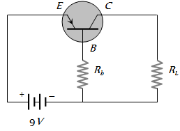
In the CB mode of a transistor, when the collector voltage is changed by 0.5 volt. The collector current changes by 0.05 mA. The output resistance will be
  • 10 kW
  • B
     20 kW
  • C
    5 kW
  • D
     2.5 kW
Answer
Correct option: A.
10 kW
 10 kW
View full question & answer
MCQ 1571 Mark
Which logic gate is represented by following diagram
  •  AND
  • B
     OR
  • C
     NOR
  • D
    XOR
Answer
Correct option: A.
 AND
 AND
View full question & answer
MCQ 1581 Mark
This symbol represents
  •  NOT gate
  • B
     OR gate
  • C
     AND gate
  • D
     NOR gate
Answer
Correct option: A.
 NOT gate
 NOT gate
View full question & answer
MCQ 1591 Mark
The Boolean equation of NOR gate is
  • A
    $C=A+B$
  • $C =\overline{ A + B }$
  • C
    $C = A \times B$
  • D
    $C =\overline{ A \cdot B }$
Answer
Correct option: B.
$C =\overline{ A + B }$
(b) $C=\overline{A+B}$
View full question & answer
MCQ 1601 Mark
If A and B are two inputs in AND gate, then AND gate has an output of 1 when the values of A and B are
  • A
     A = 0, B = 0
  •  A = 1, B = 1
  • C
     A = 1, B = 0
  • D
     A = 0, B = 1
Answer
Correct option: B.
 A = 1, B = 1
 A = 1, B = 1
View full question & answer
MCQ 1611 Mark
The given truth table is of
  • A
    OR gate
  • B
    AND gate
  • NOT gate
  • D
    None of above
Answer
Correct option: C.
NOT gate
(c) NOT gate
View full question & answer
MCQ 1651 Mark
A gate has the following truth table
P 1 1 0 0
Q 1 0 1 0
R 1 0 0 0
The gate is
  • A
     NOR
  • B
     OR
  • C
     NAND
  •  AND
Answer
Correct option: D.
 AND
AND
View full question & answer
MCQ 1661 Mark
A logic gate is an electronic circuit which
  •  Makes logic decisions
  • B
     Allows electrons flow only in one direction
  • C
     Works binary algebra
  • D
    Alternates between 0 and 1 values
Answer
Correct option: A.
 Makes logic decisions
 Makes logic decisions
View full question & answer
MCQ 1671 Mark
The logic behind ‘NOR’ gate is that it gives
  •  High output when both the inputs are low
  • B
     Low output when both the inputs are low
  • C
     High output when both the inputs are high
  • D
     None of these
Answer
Correct option: A.
 High output when both the inputs are low
High output when both the inputs are low
View full question & answer
MCQ 1681 Mark
Boolean algebra is essentially based on
  • A
    Truth
  •  Logic
  • C
     Symbol
  • D
     Numbers
Answer
Correct option: B.
 Logic
Logic
View full question & answer
MCQ 1691 Mark
The truth table shown in figure is for
A 0 0 1 1
B 0 1 0 1
y 1 0 0 1
  • A
     XOR
  • B
     AND
  • XNOR
  • D
     OR
Answer
Correct option: C.
XNOR
XNOR
View full question & answer
MCQ 1701 Mark
Given below are four logic gate symbol (figure). Those for OR, NOR and NAND are respectively
  • A
    1, 4, 3
  • B
    4, 1, 2
  • 1, 3, 4
  • D
    4, 2, 1
Answer
Correct option: C.
1, 3, 4
(c) 1, 3, 4
View full question & answer
MCQ 1711 Mark
In a transistor in CE configuration, the ratio of power gain to voltage gain is
  • A
     a
  • B
    b / a
  • C
    ba
  • b
Answer
Correct option: D.
b
b
View full question & answer
MCQ 1721 Mark
NPN transistor are preferred to PNP transistor because they have
  • A
     Low cost
  • B
    Low dissipation energy
  • C
    Capability of handing large power
  • Electrons having high mobility than holes
Answer
Correct option: D.
Electrons having high mobility than holes
View full question & answer
MCQ 1731 Mark
In NPN transistor the collector current is 10 mA. If 90% of electrons emitted reach the collector, then
  • A
    Emitter current will be 9 mA
  • Emitter current will be 11.1 mA
  • C
    Base current will be 0.1 mA
  • D
    Base current will be 0.01 mA
Answer
Correct option: B.
Emitter current will be 11.1 mA
View full question & answer
MCQ 1741 Mark
Consider an NPN transistor amplifier in common-emitter configuration. The current gain of the transistor is 100. If the collector current changes by 1 mA, what will be the change in emitter current
  • A
     1.1 mA
  • 1.01 mA
  • C
    0.01 mA
  • D
    10 mA
Answer
Correct option: B.
1.01 mA
1.01 mA
View full question & answer
MCQ 1751 Mark
While a collector to emitter voltage is constant in a transistor, the collector current changes by $8.2 mA$ when the emitter current changes by $8.3 mA.$ The value of forward current ratio $h_{fe}$ is
  • $82$
  • B
    $83$
  • C
    $8.2$
  • D
    $8.3$
Answer
Correct option: A.
$82$
$82$
View full question & answer
MCQ 1761 Mark
Which of the following is used to produce radio waves of constant amplitude
  •  Oscillator
  • B
    FET
  • C
    Rectifier
  • D
    Amplifier
Answer
Correct option: A.
 Oscillator
 Oscillator
View full question & answer
MCQ 1771 Mark
In an $\ce{NPN}$ transistor circuit, the collector current is $10 \ mA.$ If $90\%$ of the electrons emitted reach the collector, the emitter current $(i_E)$ and base current $(i_B)$ are given by
  • A
    $ \mathrm{i}_{\mathrm{E}}=-1 \mathrm{~mA}, \mathrm{i}_{\mathrm{B}}=9 \mathrm{~mA} $
  • B
    $ \mathrm{i}_{\mathrm{E}}=9 \mathrm{~mA}, \mathrm{i}_{\mathrm{B}}=-1 \mathrm{~mA} $
  • C
    $ \mathrm{i}_{\mathrm{E}}=1 \mathrm{~mA}, \mathrm{i}_{\mathrm{B}}=11 \mathrm{~mA} $
  • $ \mathrm{i}_{\mathrm{E}}=11 \mathrm{~mA}, \mathrm{i}_{\mathrm{B}}=1 \mathrm{~mA}$
Answer
Correct option: D.
$ \mathrm{i}_{\mathrm{E}}=11 \mathrm{~mA}, \mathrm{i}_{\mathrm{B}}=1 \mathrm{~mA}$
View full question & answer
MCQ 1781 Mark
If $l_1, l_2, l_3$ are the lengths of the emitter, base and collector of a transistor then
  • A
     $l_1=l_2=l_3$
  • B
     $l_3 < l_2 < l_1$
  • C
    $l_3 < l_1 < l_2$
  • $l_3 > l_1 > l_2$
Answer
Correct option: D.
$l_3 > l_1 > l_2$
$l_3 > l_1 > l_2$
View full question & answer
MCQ 1791 Mark
When NPN transistor is used as an amplifier
  • A
     Electrons move from base to emitter
  •  Electrons move from emitter to base
  • C
    Electrons moves from base to emitter
  • D
     Holes moves from base to emitter
Answer
Correct option: B.
 Electrons move from emitter to base
 Electrons move from emitter to base
View full question & answer
MCQ 1801 Mark
The relation between $a$ and $b$ parameters of current gains for a transistors is given by
  • A
     $\alpha=\frac{\beta}{1-\beta}$
  •  $\alpha=\frac{\beta}{1+\beta}$
  • C
    $\alpha=\frac{1-\beta}{\beta}$
  • D
     $\alpha=\frac{1+\beta}{\beta}$
Answer
Correct option: B.
 $\alpha=\frac{\beta}{1+\beta}$
$\alpha=\frac{\beta}{1+\beta}$
View full question & answer
MCQ 1811 Mark
For a transistor, in a common emitter arrangement, the alternating current gain $b$ is given by
  • $\beta=\left(\frac{\Delta I }{\Delta I _{ B }}\right)_{ vc }$
  • B
     $\beta=$ $\left(\frac{\Delta I _{ E }}{\Delta I _{ C }}\right)_{ v c }$
  • C
     $\beta=\left(\frac{\Delta I _{ c }}{\Delta I _{ E }}\right)_{ v c }$
  • D
     $\beta=\left(\frac{\Delta II _{ E }}{\Delta IC _{ C }}\right)_{ v c }$
Answer
Correct option: A.
$\beta=\left(\frac{\Delta I }{\Delta I _{ B }}\right)_{ vc }$
$\beta=\left(\frac{\Delta I _{ C }}{\Delta I _{ B }}\right)_{ vc }$
View full question & answer
MCQ 1821 Mark
Which of these is unipolar transistor
  • A
    Point contact transistor
  • Field effect transistor
  • C
    PNP transistor
  • D
    None of these
Answer
Correct option: B.
Field effect transistor
View full question & answer
MCQ 1831 Mark
In a transistor configuration b-parameter is
  • A
     $\frac{l_b}{1_c}$
  • $\frac{l_{ c }}{1_b}$
  • C
     $\frac{l_{ c }}{1_{ a }}$
  • D
    $\frac{1_{ a }}{1_{ c }}$
Answer
Correct option: B.
$\frac{l_{ c }}{1_b}$
View full question & answer
MCQ 1841 Mark
In a transistor, a change of 8.0 mA in the emitter current produces a change of 7.8 mA in the collector current. What change in the base current is necessary to produce the same change in the collector current
  • A
    50 mA
  • B
    100 mA
  • C
    150 mA
  • 200 mA
Answer
Correct option: D.
200 mA
200 mA
View full question & answer
MCQ 1851 Mark
In a transistor circuit shown here the base current is 35 mA. The value of the resistor $\mathrm{R}_{\mathrm{b}}$ is
  • A
    123.5 kW
  • 257 kW
  • C
    380.05 kW
  • D
    None of these
Answer
Correct option: B.
257 kW
(b) 257 kW
View full question & answer
MCQ 1861 Mark
In case of NPN-transistors the collector current is always less than the emitter current because
  • A
    Collector side is reverse biased and emitter side is forward biased
  • After electrons are lost in the base and only remaining ones reach the collector
  • C
    Collector side is forward biased and emitter side is reverse biased
  • D
    Collector being reverse biased attracts less electrons
Answer
Correct option: B.
After electrons are lost in the base and only remaining ones reach the collector
View full question & answer
MCQ 1871 Mark
In a common base amplifier circuit, calculate the change in base current if that in the emitter current is 2 mA and a = 0.98
  • 0.04 mA
  • B
    1.96 mA
  • C
    0.98 mA
  • D
    2 mA
Answer
Correct option: A.
0.04 mA
0.04 mA
View full question & answer
MCQ 1881 Mark
For a transistor, the current amplification factor is 0.8. The transistor is connected in common emitter configuration. The change in the collector current when the base current changes by 6 mA is
  • A
    6 mA
  • B
    4.8 mA
  • 24 mA
  • D
    8 mA
Answer
Correct option: C.
24 mA
24 mA
View full question & answer
MCQ 1891 Mark
The part of a transistor which is heavily doped to produce a large number of majority carriers, is
  • A
    Base
  • Emitter
  • C
    Collector
  • D
    None of these
Answer
Correct option: B.
Emitter
Emitter
View full question & answer
MCQ 1901 Mark
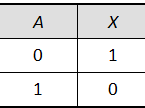
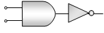
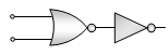
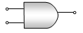
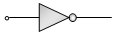
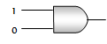
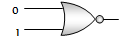
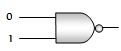
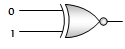
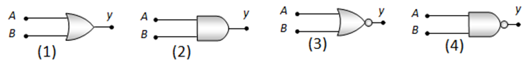
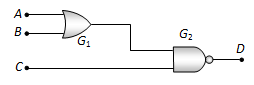
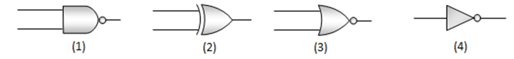
For the given combination of gates, if the logic states of inputs A, B, C are as follows A = B = C = 0 and A = B = 1, C = 0 then the logic states of output D are
  • A
    0, 0
  • B
     0, 1
  • C
     1, 0
  •  1, 1
Answer
Correct option: D.
 1, 1
1, 1
View full question & answer
MCQ 1911 Mark
An NPN-transistor circuit is arranged as shown in figure. It is
  • A
     A common base amplifier circuit
  •  A common emitter amplifier circuit
  • C
     A common collector amplifier circuit
  • D
     Neither of the above
Answer
Correct option: B.
 A common emitter amplifier circuit
 A common emitter amplifier circuit
View full question & answer
MCQ 1921 Mark
The most commonly used material for making transistor is
  • A
    Copper
  • Silicon
  • C
    Ebonite
  • D
    Silver
Answer
Correct option: B.
Silicon
Silicon
View full question & answer
MCQ 1931 Mark
The combination of ‘NAND’ gates shown here under (figure) are equivalent to
  •  An OR gate and an AND gate respectively
  • B
     An AND gate and a NOT gate respectively
  • C
     An AND gate and an OR gate respectively
  • D
     An OR gate and a NOT gate respectively.
Answer
Correct option: A.
 An OR gate and an AND gate respectively
 An OR gate and an AND gate respectively
View full question & answer
MCQ 1941 Mark
The symbol given in figure represents
  • NPN transistor
  • B
    PNP transistor
  • C
    Forward biased PN junction diode
  • D
    Reverse biased NP junction diode
Answer
Correct option: A.
NPN transistor
(a) NPN transistor
View full question & answer
MCQ 1951 Mark
A common emitter amplifier is designed with NPN transistor (a = 0.99). The input impedance is 1 KW and load is 10 KW. The voltage gain will be
  • A
     9.9
  • B
    99
  •  990
  • D
     9900
Answer
Correct option: C.
 990
990
View full question & answer
MCQ 1961 Mark
Given below are symbols for some logic gates

The XOR gate and NOR gate respectively are
  • A
    1 and 2
  •  2 and 3
  • C
     3 and 4
  • D
     1 and 4
Answer
Correct option: B.
 2 and 3
2 and 3
View full question & answer
MCQ 1971 Mark
In a PNP transistor the base is the N-region. Its width relative to the P-region is
  • Smaller
  • B
    Larger
  • C
    Same
  • D
    Not related
Answer
Correct option: A.
Smaller
Smaller
View full question & answer
MCQ 1981 Mark
A transistor is used in common emitter mode as an amplifier. Then
  • A
    The base-emitter junction is forward biased
  • B
    The base-emitter junction is reverse biased
  • C
    The input signal is connected in series with the voltage applied to the base-emitter junction
  • a, c
Answer
Correct option: D.
a, c
a, c
View full question & answer
MCQ 1991 Mark
For a transistor the parameter b = 99. The value of the parameter a is
  • A
    0.9
  • 0.99
  • C
    1
  • D
    9
Answer
Correct option: B.
0.99
0.99
View full question & answer
MCQ 2001 Mark
The transfer ratio of a transistor is 50. The input resistance of the transistor when used in the common-emitter configuration is 1 KW. The peak value for an A.C input voltage of 0.01 V peak is
  • A
    100 mA
  • B
    0.01 mA
  • C
    0.25 mA
  • 500 mA
Answer
Correct option: D.
500 mA
500 mA
View full question & answer
M.C.Q (1 Marks) - Page 4 - Physics STD 12 Science Questions - Vidyadip