Question 13 Marks
Explain the application of $p-n$ junction diode as a full-wave rectifier.
Answer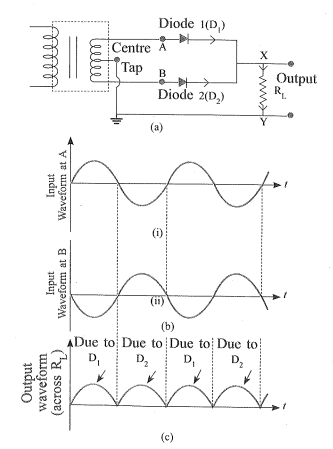
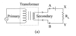
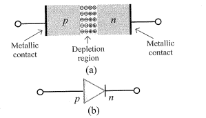
→The circuit diagram of the full-wave rectifier is shown in the figure. In full wave rectifier, two $p-n$ junction diodes are used.
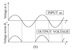
→In this type of rectifier, the rectified output voltage is obtained during both the positive as well as negative half of ac cycle. Hence, it is known as full-wave rectifier.
→As shown in fig., the $p$-side of the two diodes are connected to the ends of the secondary of the transformer. The $n$-side of the diodes are connected together and the output is taken between this common point of diodes and the mid-point of the secondary of the transformer. So for a full wave rectifier the secondary of the transformer is provided with a centre tapping and so it is called centre-tap transformer.
→As can be seen from fig. (c), the voltage rectified by each diode is only half the total secondary voltage. Each diode rectifies only for half the cycle, but the two do so for alternate cycles. Thus the output between their common terminals and the centre tap of the transformer becomes a full-wave rectifier output.
→Suppose the input voltage to A with respect to centre tap at any instant is positive. At that instant, voltage B being out of phase should be negative. In this case, diode $D _1$ gets forward biased and conducts, while $D _2$ gets reverse biased and does not conduct. Hence, as shown in fig. c, output current is obtained between two terminals of $R _{ L }$ during this half-cycle.
→During the other half-cycle, voltage at A is negative and voltage at B is positive. In this case diode $D_1$ is in reverse bias condition and $D_2$ is in forward bias. Hence, in this part of cycle, $D _2$ conducts and output voltage is obtained.
→Thus, we get output voltage during both positive as well as negative half of the cycle.
View full question & answer→→The circuit diagram of the full-wave rectifier is shown in the figure. In full wave rectifier, two $p-n$ junction diodes are used.
→In this type of rectifier, the rectified output voltage is obtained during both the positive as well as negative half of ac cycle. Hence, it is known as full-wave rectifier.
→As shown in fig., the $p$-side of the two diodes are connected to the ends of the secondary of the transformer. The $n$-side of the diodes are connected together and the output is taken between this common point of diodes and the mid-point of the secondary of the transformer. So for a full wave rectifier the secondary of the transformer is provided with a centre tapping and so it is called centre-tap transformer.
→As can be seen from fig. (c), the voltage rectified by each diode is only half the total secondary voltage. Each diode rectifies only for half the cycle, but the two do so for alternate cycles. Thus the output between their common terminals and the centre tap of the transformer becomes a full-wave rectifier output.
→Suppose the input voltage to A with respect to centre tap at any instant is positive. At that instant, voltage B being out of phase should be negative. In this case, diode $D _1$ gets forward biased and conducts, while $D _2$ gets reverse biased and does not conduct. Hence, as shown in fig. c, output current is obtained between two terminals of $R _{ L }$ during this half-cycle.
→During the other half-cycle, voltage at A is negative and voltage at B is positive. In this case diode $D_1$ is in reverse bias condition and $D_2$ is in forward bias. Hence, in this part of cycle, $D _2$ conducts and output voltage is obtained.
→Thus, we get output voltage during both positive as well as negative half of the cycle.