Questions · Page 4 of 5

M.C.Q (1 Marks)

MCQ 1511 Mark
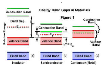
Energy gaps between the highest band and the lowest empty bands in elements $A, B, C$ and $D$ are $0,70,530$ and $90 \ kJ\ mol−1.$ Then,
  • A
    Element $A$ is metal
  • B
    Element $C$ is insulator
  • C
    Element $B$ and $D$ can be semiconductors
  • All are correct conclusion about elements $A, B, C$ and $D$
Answer
Correct option: D.
All are correct conclusion about elements $A, B, C$ and $D$
Energy gaps between the highest band and the lowest empty bands is lowest in metals, moderate in semi conductors and very high in insulators. This suggests us that:
Element $A$ must be a metal, element $C$ must be an insulator and element $B$ and $D$ can be semiconductors.
View full question & answer
MCQ 1521 Mark
Let $n_p$ and $n_e$ be the number of holes and conduction electrons in an intrinsic semiconductor.
  • A
    $\text{n}_\text{p} > \text{n}_\text{e}$
  • $\text{n}_\text{p} = \text{n}_\text{e}$
  • C
    $\text{n}_\text{p} < \text{n}_\text{e}$
  • D
    $\text{n}_\text{p}\neq\text{n}_\text{e}$
Answer
Correct option: B.
$\text{n}_\text{p} = \text{n}_\text{e}$
As the intrinsic semiconductor is free from all impurities, the number of electrons is equal to the number of holes.
View full question & answer
MCQ 1531 Mark
The energy gap in case of which of the following is less than $3\ eV$?
  • A
    Aluminium
  • B
    Iron
  • Germanium
  • D
    Copper
Answer
Correct option: C.
Germanium
Energy gap of most of the semiconductors is nearly $1.1\ eV$ which is less than $3\ eV$.
As we know germanium is a semiconductor and its energy gap is $0.67\ eV$. Thus germanium is the right answer.
View full question & answer
MCQ 1541 Mark
The vacancy created due to the absence of an electron in the valence band of a semiconductor is called a $.........$
  • A
    Electron
  • Hole
  • C
    Proton
  • D
    Position
Answer
Correct option: B.
Hole
Whenever an electron jumps from a valence band to conduction band, an equal and opposite charge is left behind in the place of an electron. This is called a hole.
View full question & answer
MCQ 1551 Mark
A hole is :
  • A
    A positively charged electron.
  • B
    An electron in the valence band.
  • An unfilled covalent bond.
  • D
    An excess electron in covalent bond.
Answer
Correct option: C.
An unfilled covalent bond.
When the covalent bond breaks, electrons are freed from atom. The departure of electron from valence band creates vacancy in bond, this vacancy is known as hole. Hence, a hole is an unfilled covalent bond.
View full question & answer
MCQ 1561 Mark
What happens during regulation action of a Zener diode?
  • A
    The current in and voltage across the Zenor remains fixed.
  • B
    The current through the series Resistance ($\mathrm{R}_{\mathrm{s}}$) changes.
  • C
    The resistance offered by the Zener changes.
  • B and C both
Answer
Correct option: D.
B and C both
Solution:
Symbolically zener diode represents like this:
In the forward bias, the zener diode acts as an ordinary diode. It can be used as a voltage regulator.

A zener diode when reverse biases offers constant voltage drop across in terminals as unregulated voltage is applied across circuit to regulate. Then during regulation action of a Zener diode, the current through the series resistance $\mathrm{R}_{\mathrm{s}}$ changes and resistance offered by the Zener changes. The current through the Zener changes but the voltage across the Zener remains constant.
View full question & answer
MCQ 1571 Mark
Forward biasing is that in which applied voltage :
  • A
    Increases potential barrier.
  • Cancels the potential barrier.
  • C
    Is equal to $1.5$volt.
  • D
    None of these.
Answer
Correct option: B.
Cancels the potential barrier.
View full question & answer
MCQ 1581 Mark
The energy band gap $($distance between the conduction band and valence band$)$ in conductor is.
  • $0$
  • B
    $4\mathring{\text{A}}$
  • C
    $10\mathring{\text{A}}$
  • D
    $100\mathring{\text{A}}$
Answer
Correct option: A.
$0$
In conductors, the valence band and conduction band overlap each other or have the extremely small energy gap between them approximately equal to zero.
View full question & answer
MCQ 1591 Mark
What is the resistivity of a pure semiconductor at absolute zero?
  • A
    Zero.
  • Infinity.
  • C
    Same as that of conductors at room temperature.
  • D
    Same as that of insulators at room temperature.
Answer
Correct option: B.
Infinity.
View full question & answer
MCQ 1601 Mark
The mobility of free electrons is greater than that of free holes because:
  • A
    They are light.
  • B
    They carry negative charge.
  • C
    They mutually colllide less.
  • They require low energy to continue their motion.
Answer
Correct option: D.
They require low energy to continue their motion.
View full question & answer
MCQ 1611 Mark
For detecting the light $.........$
  • A
    The photodiode has to be forward biased.
  • The photodiode has to be reversed biased.
  • C
    The $\text{LED}$ has to connected in forward bias mode.
  • D
    The $\text{LED}$ has to be connected in reverse bias mode.
Answer
Correct option: B.
The photodiode has to be reversed biased.
Photo diode is used to detect light.
In reverse biased condition, the width of depletion region increases as the the applied reverse bias voltage increases across the diode. So, by applying a larger voltage, more of the incident photons are converted to electric current thereby increasing the efficiency.
In forward biased condition, the width of depletion region decreases so only a small portion of the incident photons get converted to electric current and hence the efficiency is less.
Hence photo diode in reverse biased condition detects light.
View full question & answer
MCQ 1621 Mark
In the valance band, the current is due to :
  • A
    The presence of electrons
  • The presence of holes
  • C
    The presence of both electrons and holes
  • D
    None of the above
Answer
Correct option: B.
The presence of holes
In the valence band, current is only due to holes. In the conduction band, current is due to electrons.
View full question & answer
MCQ 1631 Mark
A semiconducting device is connected in a series circuit with a battery and a resistance. A current is found to pass through the circuit. If the polarity of the battery is reversed, the current drops to almost zero. the device may be :
  • A
    An intrinsic semiconductor.
  • B
    A $p-$type semiconductor.
  • C
    An $n-$type semiconductor.
  • A $p-n$ junction.
Answer
Correct option: D.
A $p-n$ junction.
As a $p−n$ junction allows the flow of current in forward bias and stops the current in reverse bias $($almost negligible reverse leakage current flows in the reverse$-$biassed $p−$njunction$)$, the device should be a $p−n$ junction. Other options are examples of semiconductors that allow moderate current to flow and that do not have any effect of changing the polarity of the battery.
View full question & answer
MCQ 1641 Mark
Electric conduction in a semiconductor takes place due to :
  • A
    Electrons only.
  • B
    Holes only.
  • Both electrons and holes.
  • D
    Neither electrons nor holes.
Answer
Correct option: C.
Both electrons and holes.
View full question & answer
MCQ 1651 Mark
What is the order of magnitude of the resistance of a dry human body?
  • A
    $10\Omega$  
  • $10^4\Omega $
  • C
    $10 M\Omega$
  • D
    $10\mu \Omega$
Answer
Correct option: B.
$10^4\Omega $
It is known that the resistance of a dry human body is $10k\Omega = 10^4\Omega $.
View full question & answer
MCQ 1661 Mark
The battery connections required to forward bias a $pn$ junction are $.........$
  • $+ve$ terminal to $p$ and $-ve$ terminal to $n$
  • B
    $-ve$ terminal to $p$ and $+ve$ terminal to $n$
  • C
    $-ve$ terminal to $p$ and $-ve$ terminal to $n$
  • D
    None of these
Answer
Correct option: A.
$+ve$ terminal to $p$ and $-ve$ terminal to $n$
To forward bias the $p-n$ junction, the $p$ side is made more positive, so that it is "downhill" for electron motion across the junction. An electron can move across the junction and fill a vacancy or "hole" near the junction. It can then move from vacancy to vacancy leftward toward the positive terminal, which could be described as the hole moving right. The conduction direction for electrons in the diagram is right to left, and the upward direction represents increasing electron energy.

View full question & answer
MCQ 1671 Mark
A $220 V A.C$. supply is connected between points $A$ and $B ($Fig.$)$. What will be the potential difference $V$ across the capacitor?
  • A
    $220V.$
  • B
    $110V.$
  • C
    $0V.$
  • $220\sqrt{2}\text{V}.$
Answer
Correct option: D.
$220\sqrt{2}\text{V}.$
Key concept: Half wave rectifier: When the $P-N$ junction diode rectifies half of the ac wave, it is called half wave rectifier.

  1. During positive half cycle,
Diode $\rightarrow$ Forward biased
Output signal $\rightarrow$ obtained
  1. During negative half cycle,
Diode $\rightarrow$ reverse biased
Output signal $\rightarrow$ not obtained
  1. Output voltage is obtained across the load resistance $RL$. It is not constant but pulsating $($mixture of ac and $dc)$ in nature.
  2. Average output in one cycle
$\text{I}_\text{dc}=\frac{\text{I}_0}{\pi}\text{ and }\text{V}_\text{dc}=\frac{\text{V}_0}{\pi};\text{I}_0=\frac{\text{V}_0}{\text{r}_\text{f}+\text{R}_\text{I}}$
$(rf =$ forward biased resistance$)$
  1. $r.m.s$. output: $\text{I}_\text{rms}=\frac{\text{I}_0}{2},\text{V}_\text{rms}=\frac{\text{V}_0}{2}$
As $p-n$ junction diode will consuct during positive half cycle only, during negative half cycle diode is reverse biased. During this diode will not give any output. So, potential difference across capacitor $C =$ peak voltage of the given $AC$ voltage
$=\text{V}_0=\text{V}_\text{rms}\sqrt{2}=220\sqrt{2}\text{V}$
View full question & answer
MCQ 1681 Mark
Zener diode works on:
  • A
    Zero bias
  • Reverse bias
  • C
    Forward bias
  • D
    Infinite bias
Answer
Correct option: B.
Reverse bias
We know that zener diode works on the reverse bias. When the reverse bias is equal to the break$-$down voltage, the voltage across the zener remains almost constant and the current increases rapidly.
View full question & answer
MCQ 1691 Mark
Which logic gate produces $\text{LOW}$ output when any of the inputs is $\text{HIGH}$?
  • A
    $\text{AND}$
  • B
    $OR$
  • C
    $\text{NAND}$
  • $\text{NOR}$
Answer
Correct option: D.
$\text{NOR}$
The truth table for $\text{NOR}$ gate is shown above which suggests that $\text{NOR}$ gate is the logic gate which produces low output when any of the inputs is high.
View full question & answer
MCQ 1701 Mark
Which of the following logic gates is an universal gate?
  • A
    $\text{OR}$
  • B
    $\text{NOT}$
  • C
    $\text{AND}$
  • $\text{NOR}$
Answer
Correct option: D.
$\text{NOR}$
$\text{NAND}$ gate is considered universal gate. As other gates can be formed from this gate.
View full question & answer
MCQ 1711 Mark
One serious drawback of semi$-$conductor devices is:
  • A
    They do not last for long time.
  • B
    They are costly.
  • They cannot be used with high voltage.
  • D
    They pollute the environment.
Answer
Correct option: C.
They cannot be used with high voltage.
View full question & answer
MCQ 1721 Mark
$p-n$ junction diode acts as:
  • A
    ohmic resistance
  • non$-$ohmic resistance
  • C
    both $A$ and $B$
  • D
    amplifier
Answer
Correct option: B.
non$-$ohmic resistance
We know that in the case of metallic conductors, the potential difference varies in direct proportion to the current flowing. The $I−V$ graph of a ohmic conductor is a straight line. But, a $p-n$ junction diode is not in according with Ohm's law. The current voltage characteristic curve of a $p-n$ junction diode shows both forward bias as well as reverse bias characteristics as shown as in the graph.
View full question & answer
MCQ 1731 Mark
In the depletion region of a $pn$ junction, there is a shortage of:
  • A
    Acceptor ions
  • Holes and electrons
  • C
    Donor ions
  • D
    None of these
Answer
Correct option: B.
Holes and electrons
Depletion region of a $p-n$ junction is formed due to the shortage of holes and electrons.
View full question & answer
MCQ 1741 Mark
Zener diode is used for:
  • A
    Amplification
  • B
    Rectification
  • Stabilisation
  • D
    All of the above
Answer
Correct option: C.
Stabilisation
A zener diode is always operated in its reverse biased condition. A voltage regulator circuit can be designed using a zener diode to maintain a constant $DC$ output voltage across the load in spite of variations in the input voltage or changes in the load current. The zener voltage regulator consists of a current limiting resistor $RS$​ connected in series with the input voltage $VS$​ with the zener diode connected in parallel with the load $RL$ in this reverse biased condition.Hence we can say that ,zener diode is used for stabilization.

View full question & answer
MCQ 1751 Mark
The electrical conductivity of pure germanium can be increased by:
  • A
    Increasing the temperature.
  • B
    Doping acceptor impurities.
  • C
    Doping donor impurities.
  • All of the above.
Answer
Correct option: D.
All of the above.
View full question & answer
MCQ 1761 Mark
The creation of voltage or electric current in a material upon exposure to light is termed as :
  • A
    Photo$-$ionic effect
  • B
    Thermi$-$ionic effect
  • Photo$-$voltaic effect
  • D
    None of these.
Answer
Correct option: C.
Photo$-$voltaic effect
The generation of current or voltage in a material, when exposed to light is called photovoltaic effect.
The device which operates on this effect is called photo$-$voltaic device or solar cell. It is a $p-n$ junction diode which converts solar energy into electrical energy.
View full question & answer
MCQ 1771 Mark
In physics, chemistry, and electronic engineering, $.........$ is the lack of an electron at a position where one could exist in an atom or atomic lattice.
  • An electron hole
  • B
    Electron
  • C
    Proton
  • D
    Neutron
Answer
Correct option: A.
An electron hole
A hole is an absence of an electron in a particular place in an atom. Although it is not a physical particle, a hole can be passed from atom to atom in a semiconductor material.
View full question & answer
MCQ 1781 Mark
Which of these is the best description of a Zener diode?
  • It is a constant voltage device.
  • B
    It operates in the reverse region.
  • C
    It is a constant current device.
  • D
    It works in forward region.
Answer
Correct option: A.
It is a constant voltage device.
Zener diode is a $p-n$ junction diode working in the breakdown region. It is used as a voltage regulator$/$stabilizer to provide a constant voltage from a source whose voltage may fluctuate over a wide range.
View full question & answer
MCQ 1791 Mark
Digital circuit can be made by repetitive use of this gate:
  • A
    $\text{AND}$
  • B
    $\text{OR}$
  • C
    $\text{NOT}$
  • $\text{NAND}$
Answer
Correct option: D.
$\text{NAND}$
$\text{NAND}$ and $\text{NOR}$ gates are the basic building blocks of the digital circuit which means that all other gates can be synthesized using $\text{NAND} ($or $\text{NOR)}$ gate only.
View full question & answer
MCQ 1801 Mark
The expression of $Y$ in the above circuit is:
  • A
    $\text{ABCD}$
  • B
    $\text{A+BCD}$
  • $\text{A+B+C+D}$
  • D
    $\text{AB+CD}$
Answer
Correct option: C.
$\text{A+B+C+D}$
Here, to build the logic three $\text{OR}$ gates are used hence, all the input signals will be added to each other
Hence, the boolean expression is : $\text{A+B+C+D = Y}$
View full question & answer
MCQ 1811 Mark
An electric field is applied to a semiconductor. Let the number of charge carriers be $n$ and the average drift speed be $v$. If the temperature is increased,
  • A
    Both $n$ and $u$ will increase.
  • $n$ will increase but $v$ will decrease.
  • C
    $v$ will increase but $n$ will decrease.
  • D
    Both $n$ and $v$ will decrease.
Answer
Correct option: B.
$n$ will increase but $v$ will decrease.
As we increase the temperature, additional electron$‒$hole pairs are created in a semiconductor. As a result, the number of charge carriers increases.
Now, drift velocity $(v_d)$ is given by
$\text{vd}=\frac{-\text{eE}_\text{T}}{\text{m}}$
As the temperature increases, the relaxation time of charge carriers $(T)$ decreases. As a result, $v_d$ decreases.
View full question & answer
MCQ 1821 Mark
A pure semiconductor at absolute zero has :
  • A
    Absence of electrons in the conduction band.
  • B
    All the electrons occupying the valence band.
  • C
    Large $E_g$​ value.
  • All of the above.
Answer
Correct option: D.
All of the above.
At absolute zero temperature, in a pure semiconductor, all electrons occupy the valence band and no electrons are present in the conduction band. The forbidden gap energy $E_g$​ is large.
View full question & answer
MCQ 1831 Mark
Temperature coefficient of resistance of semiconductor is :
  • A
    Zero.
  • B
    Constant.
  • C
    Positive.
  • Negative.
Answer
Correct option: D.
Negative.
View full question & answer
MCQ 1841 Mark
A Zener diode :
  • A
    Is a lightly doped junction diode.
  • Heavily doped junction diode.
  • C
    Is either $p-$type or $n-$type.
  • D
    Has no $p-n$ junction.
Answer
Correct option: B.
Heavily doped junction diode.
The reverse breakdown voltage depends on doping of the diode. Hence, in the Zener diode the heavy doping of its $p-n$ junction is done. The depletion region formed in the diode is very thin $(<1 m)$ and the reverse bias voltage of about $5 V$ which is less than ordinary diode.
View full question & answer
MCQ 1851 Mark
The zone in a semiconductor diode where no free charge carriers exists is known as the :
  • A
    Anode region
  • B
    Cathode region
  • Depletion region
  • D
    None of these
Answer
Correct option: C.
Depletion region
In depletion region negative charge carrier electrons are attached with their positive charge carrier holes. hence there is no free charge carriers exists.
View full question & answer
MCQ 1861 Mark
The output of a $2-$input $\text{OR}$ gate is zero only when its :
  • Both inputs are $0$.
  • B
    Either input is $1.$
  • C
    Both inputs are $1.$
  • D
    Either input is $0.$
Answer
Correct option: A.
Both inputs are $0$.
The truth table for $2-$input $\text{OR}$ gate is as shown in the figure. Thus, the output is zero only when both inputs are zero.
View full question & answer
MCQ 1871 Mark
There is no hole current in conductors, because they have :
  • A
    High conductivity
  • B
    High electron density
  • C
    No valence band
  • Overlapping of valence and conduction bands.
Answer
Correct option: D.
Overlapping of valence and conduction bands.
In conductors, electrons are loosely bound to the nucleus hence, can detach easily at room temperature. Also, a large number of free electrons thus, available are conduction electrons. When the covalent bond breaks, electrons are freed from the atom.
The departure of an electron from valence band creates the vacancy in bond, this vacancy is known as hole. This hole is captured by another free electron.
Also, the energy level of free electrons corresponds to the conduction level, hence valance level and conduction level are overlapped. So there are no holes in conduction level to carry hole current.
View full question & answer
MCQ 1881 Mark
An intrinsic semiconductor is                         :
  • Undoped
  • B
    Doped
  • C
    Can be undoped or doped
  • D
    Semi$-$doped
Answer
Correct option: A.
Undoped
Doping is a process of adding impurities in a semiconductor. Doped semiconductors are known as extrinsic semiconductors and others are known as intrinsic ones.
View full question & answer
MCQ 1891 Mark
Which of the following contains a covalent bond?
  • A
    Copper
  • B
    $\text{NaCl}$
  • Germanium
  • D
    Helium
Answer
Correct option: C.
Germanium
A covalent bond is a chemical bond that involves the sharing of electron pairs between atoms. The stable balance of attractive and repulsive forces between atoms when they share electrons is known as covalent bonding.
As the valency of germanium is $4$, it can share $4$ electrons of neighboring atom to complete the octet.
Hence, Ge has covalent bond. $\text{NaCl}$ is an example of an ionic bond and helium and copper both have valency $2$ and $1$ respectively.
View full question & answer
MCQ 1901 Mark
In an intrinsic semiconductor, if Ne​ is the number of electrons in the conduction band and $Np​$ is the number of holes in the valence band then.
  • A
    $ \mathrm{N}_{\mathrm{e}} > \mathrm{N}_{\mathrm{p}} $
  • $ \mathrm{N}_{\mathrm{e}}=\mathrm{N}_{\mathrm{p}} $
  • C
    $ \mathrm{N}_{\mathrm{e}} < \mathrm{N}_{\mathrm{p}}$
  • D
    None of the above
Answer
Correct option: B.
$ \mathrm{N}_{\mathrm{e}}=\mathrm{N}_{\mathrm{p}} $
In an intrinsic semiconductor, the number of electrons in the conduction band is equal to the number of holes in the valence band, so $ \mathrm{N}_{\mathrm{e}}=\mathrm{N}_{\mathrm{p}} $
View full question & answer
MCQ 1911 Mark
In an insulator, the forbidden energy gap between the valence band and conduction band is of the order of :
  • A
    $1M\ eV$
  • B
    $0.1M\ eV$
  • C
    $1\ eV$
  • $5\ eV$
Answer
Correct option: D.
$5\ eV$
Forbidden energy gap, also known as band gap refers to the energy difference $(eV)$ between the top of valence band and the bottom of the conduction band in materials. Current flowing through the materials is due to the electron transfer from the valence band to the conduction band.
Insulators do not conduct electricity because a large amount of energy is needed for the electrons to cross the forbidden energy gap. Moreover the forbidden energy gap is the widest $(>5eV)$ in case of insulators.
Example: Forbidden energy gap in diamond is nearly $5.5\ eV.$
View full question & answer
MCQ 1921 Mark
In $n-$type of semiconductor, majority carries are:
  • A
    Positron
  • Electron
  • C
    Holes
  • D
    Impure particles
Answer
Correct option: B.
Electron
In $n-$type semiconductor, large number of free electrons is present. Hence, free electrons are the majority charge carriers in the $n-$type semiconductor. The free electrons $($majority charge carriers$)$ carry most of the electric charge or electric current in the $n-$type semiconductor.
View full question & answer
MCQ 1931 Mark
If the series resistance decreases in an unloaded zener regulator, the zener current:
  • A
    Decreases
  • B
    Stays the same
  • Increases
  • D
    Equals the voltage divided by the resistance.
Answer
Correct option: C.
Increases
current increases as the resistance decreases, as zener current is inversely proportional to the series resistance.
View full question & answer
MCQ 1941 Mark
The pn junction can be formed by which of the following methods?
  • A
    Grown junction method
  • B
    Alloying method
  • C
    Diffusion method
  • All of these
Answer
Correct option: D.
All of these
Grown Junction Diode:
Diodes of this type are formed during the crystal pulling process. $P$ and $N-$type impurities can be alternately added to the molten semiconductor material in the crucible, which results in a $P-N$ junction when crystal is pulled. After slicing, the larger area device can then be cut into a large number of smaller$-$area semiconductor diodes. Though such diodes, because of larger area, are capable of handling large currents but larger area also introduces more capacitive effects, which are undesirable. Such diodes are used for low frequencies.
Alloy Type or Fused Junction Diode: Such a diode is formed by first placing a $P-$ type impurity $($a tiny pellet of aluminium or some other $P-$ type impurity$)$ into the surface of an $N-$type crystal and heating the two until liquefaction occurs where the two materials meet. An alloy will result that on cooling will give a $P-N$ junction at the boundary of the alloy substrate. Similarly, an $N-$type impurity may be placed into the surface of a $P-$ type crystal and the two are heated until liquefaction occurs. Alloy type diodes have a high current rating and large $\text{PIV} ($peak inverse voltage$)$ rating. The junction capacitance is also large, due to the large junction area.
View full question & answer
MCQ 1951 Mark
In a npn transistor circuit, the collector current is 10mA. If 95 per cent of the electrons emitted reach the collector, which of the following statements are true?
  • A
    The emitter current will be 8mA.
  • B
    The emitter current will be 10.53mA.
  • C
    The base current will be 0.53mA.
  • B and C both
Answer
Correct option: D.
B and C both
Solution:
Given Ic = 10mA
According to the question, $\text{I}_\text{c}=\frac{95}{100}\text{I}_\text{e}$
$\Rightarrow\ \text{I}_\text{e}=\frac{10\times100}{95}=10.53\text{mA}$
We know that, $\mathrm{I}_{\mathrm{b}}=\mathrm{I}_{\mathrm{e}}=\mathrm{I}_{\mathrm{C}}=$ 10.53 - 10 = 0.53mA.
View full question & answer
MCQ 1961 Mark
The number $0 ($zero$)$ is required for:
  • A
    Transistor
  • B
    Abacus
  • Computer
  • D
    Calculator
Answer
Correct option: C.
Computer
The number $0$ is most important in digital communication where only two states $0,1$ control the input and output and computer is based on digital signals.
View full question & answer
MCQ 1971 Mark
In an intrinsic semiconductor, conductivity is :
  • Low at room temperature
  • B
    Average
  • C
    High at room temperature
  • D
    Zero at room temperature
Answer
Correct option: A.
Low at room temperature
In intrinsic semiconductors, $n = p$. Hence, at room temperature, no free electrons are available for conduction. If the temperature is increased, the covalent bonds will break and electrons will be freed, each electron will leave behind a hole and capture a new hole the process will continued and charge flows through intrinsic semiconductor.
Thus, its conductivity increases with temperature. Hence, in intrinsic semiconductor conductivity is low at room temperature.
View full question & answer
MCQ 1981 Mark
Zener diode is used for:
  • A
    Amplification.
  • B
    Rectification.
  • Stabilisation.
  • D
    All of the above.
Answer
Correct option: C.
Stabilisation.
View full question & answer
MCQ 1991 Mark
The transducer used in television transmission works on the principle of :
  • A
    Electromagnetic induction
  • Photoelectric effect
  • C
    Raman's effect
  • D
    Rayleigh's effect
Answer
Correct option: B.
Photoelectric effect
A transducer is an electronic device that converts light energy to electrical energy in television. When light falls on photosensitive element electric current is generated that is measured directly or after amplification. Similarly, photoelectric effect is the ejection of electrons from a metal or semiconductor surface when illuminated by light or any radiation of suitable wavelength.
View full question & answer
MCQ 2001 Mark
Conventional flow of current will always be from:
  • $p$ type $\rightarrow n$ type
  • B
    $n$ type $\rightarrow p$ type
  • C
    $n$ Type $\rightarrow n$ type
  • D
    None of these
Answer
Correct option: A.
$p$ type $\rightarrow n$ type
The holes in the covalent bonds of $p-$type semiconductor. They appear to move towards $n-$type semiconductor. Because the electrons in the covalent bonds of $n-$type semiconductor $($not free electrons$)$ jump towards $p-$type semiconductor due to plenty of holes available in the covalent bonds at $p-$side.
Hence, conventional current flow from $p-$type to $n-$type.
View full question & answer