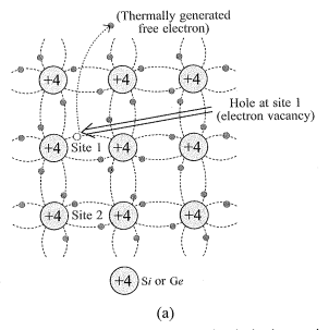
Questions

2 Marks Questions

🎯

Test yourself on this topic

21 questions · timed · auto-graded

Question 12 Marks
What is Rectifier?
Answer
From the V-I characteristic of a junction diode we see that it allows current to pass only when it is forward biased. So if an alternating voltage is applied across a diode, the current flows only in that part of the cycle when the diode is forward biased.
This property is used to rectify alternating voltages and the circuit used for this purpose is called a rectifier.
A rectifier converts AC energy in to DC energy.
View full question & answer
Question 22 Marks
Write the difference between $p$-type and n-type semiconductors.
Answer
 $p \text { - type }$
semiconductor
$n \text { - type }$
semiconductor
1.Trivalent impurity is added in pure semiconductor.Pentavalent impurity is added in pure semiconductor.
2.Exa. Boron, Al, In.Exa. Phosphorous, Antimony, Arsenic etc.
3.Holes are majority charge carriers and free electrons are the minority carriers.Free electrons are the majority charge carriers and holes are the minority carriers.
4.$n_h \gg n_e$$n_e \gg n_h$
5.Electricity conduction primarily occurs due to holes.Electricity conduction primarily occurs due to motion of electrons.
View full question & answer
Question 42 Marks
What is a filter circuit? Explain its functioning.
Answer
The rectified voltage is in the form of pulses of the shape of half sinusoilds. Though, it is unidirectional it does not have a steady value.
To get steady dc output from pulsating voltage, the filter circuit is used. Filter circuits consist of only capacitor, only inductor or a combination of both. Since these additional circuits appear to filter out the ac ripple and give a pure dc voltage, so they are called filters.
• Functioning of a Filter Circuit :
When the voltage across the capacitor is rising, it gets charged. If there is no external load, it remains charged to peak voltage of the rectified output.
When there is a load, it gets discharged through the load and the voltage across it begins to fall. In the next half cycle of rectified output it again gets charged to the peak value.
As shown in the fig., the rate of fall of the voltage across capacitor depends on the inverse product of capacitor C and the effective resistance $R_L$ used in the circuit and is called the time constant. To make the time constant large, value of C should be large. So capacitor input filters use large capacitors.
The output voltage obtained by using capacitor input filter is nearer to the peak voltage of the rectified voltage.
This type of filter is most widely used in power supplies.
Image
View full question & answer
Question 52 Marks
Write down the difference between forward bias and reverse bias of $p-n$ junction diode.
Answer
Forward BiasReverse Bias
$p$ - type semiconductor of $p-n$ junction is connected to positive terminal and $n$ - type is connected with negative terminal of battery. Such a biasing is called forward biasing.$p$ - type semiconductor of $p-n$ junction is connected to negative terminal and $n$ - type is connected with positive terminal of battery. Such a biasing is called reverse biasing.
In forward bias, the current is due to majority charge carriers.In Reverse bias, the current is due to minority charge carriers.
Current obtained in forward bias is of the order of $m A$.Current obtained in Reverse bias is of the order of $\mu A$.
When diode is connected in forward bias, width of its depletion layer and height of potential barrier reduces.When diode is connected in reverse bias, width of its depletion layer and height of potential barrier increases.
Resistance is of the order of $10 \Omega$ to $100 \Omega$.Resistance is of the order of $10 M \Omega$.
View full question & answer
Question 62 Marks
What are $V-1$ characteristics of a $p-n$ junction?
Answer
The current and voltage changes for a $p-n$ junction diode are represented by a graph. This graph is known as V-I characteristics of the diode, which are of the following two types:
(i) Forward characteristics
(ii) Reverse characteristics
View full question & answer
Question 72 Marks
Prove $n_e \cdot n_h=n_i^2$ for $n-$ type and $p-$ type semiconductors where,
$n_e - $number density of electrons
$n_h - $ number density of holes
$n_i -$ number density of intrinsic charge carriers
Answer
$\rightarrow$ The creation of electron $-$ hole pair due to the migration of the electron to the conduction band is not a very stable situation.
$\rightarrow$ The electrons and holes collide with each other as per the laws of thermodynamics and the temperature. The electrons once again occupies the hole.
$\rightarrow$ The creation of the electron hole pair and its recombination process takes place at the same time.
$\rightarrow$ In the equillibrium position the rate of electron hole pair formation and their recombination is equal.
The recombination rate $\propto n_h \cdot n_e$ recombination rate $= R \cdot n_h \cdot n_e$
Here, $R$ is known as the recombination coefficient.
$\rightarrow$ For an intrinsic $($or pure$)$ semiconductor, $n_e=n_h=n_i$
Hence the recombination rate $= R \cdot n_h \cdot n_e$
$= R n_i^2$
$\rightarrow$ But, as the crystal structures of intrinsic semiconductors and the extrinsic semiconductors are prepared from them and also because the above processes follow the laws of thermodynamics, the rate of recombination is same for both this types of semiconductors.
$\therefore R \cdot n_e \cdot n_h= R \cdot n_i^2$
$\therefore n_i^2=n_e \times n_h$
View full question & answer
Question 82 Marks
Explain $n$-type and $p$-type semiconductors on the basis of band theory.
Answer
The semiconductor's energy band structure is affected by doping. In the case of extrinsic semi-conductors, additional energy states due to donor impurities $\left( E _{ D }\right.$ ) and acceptor impurities $\left( E _{ A }\right.$ ) also exist.
Image
In the energy band diagram of $n$-type Si semiconductor, the donor energy level $E _{ D }$ is slightly below the bottom $E _{ C }$ of conduction band and the electrons from this level move into the conduction band with very small supply of energy. At room temperature, most of the donor atoms get ionised but very few ( $\sim 10^{-12}$ ) atoms of $S i$ get ionised. So the conduction band will have most electrons coming from the donor impurities as shown in fig. (a).
Similarly for $p$-type semiconductor, the acceptor energy level $E _{ A }$ is slightly above the top of $E _{ V }$ the valence band as shown in fig (b).
At room temperature, most of the acceptor atoms get ionised, which create holes in the valence band.
Thus at room temperature, the density of holes in the valence band is pre-dominantly due to impurity in the extrinsic semiconductor. The electron and hole concentration in a semiconductor in thermal equilibrium is given by,
$n_e \cdot n_h=n_i^2 \text {. }$
View full question & answer
Question 92 Marks
What is doping ? - Explain.
Answer
"The deliberate addition of a desired impurity is called doping. And the impurity atoms are called dopants. Such a material is also called a doped semiconductor (or extrinsic semiconductors or impurity semiconductors.)".
The dopant atom (impurity atom) has to be such that it does not distort the original pure semiconductor lattice.
It occupies only a very few of the original semiconductor sites in the crystal. A necessary condition to attain this is that the sizes of the dopant and the semiconductor atoms should be nearly same.
Generally a small amount, say, a few parts per million (ppm), of a suitable impurity is added to the pure semi-conductor. Due to the added impurity atoms, the conductivity of the semiconductor is increased manifold.
There are two types of dopants used in doping the tetravalent $S i$ or Ge:
(i) Pentavalent (Valency 5) : like Arsenic (As), Antimony (S $b$ ), Phosphorous ( P ), etc.
(ii) Trivalent (Valency 3) : like Indium (I $n$ ) Boron (B), Aluminium $( A l$ ) etc.
View full question & answer
Question 102 Marks
Explain the change in the Energy gap of an intrinsic semiconductor, with temperature
Answer
As shown in Fig. (a), at absolute zero temperature, all the electrons in an intrinsic semiconductor are in valence band. There are no electrons in the conduction band. This means that there are no free electrons, So, at 0 K temperature, an intrinsic semiconductor behaves like an insulator.
Image
As shown in Fig. (b), due to thermal energy at high temperature ( $T >0 K$ ), Some electrons gain energy, get in to excited state and go from valence band to conduction band.
These thermally excited electrons at $T >0 K$, partially occupy the conduction band. Therefore the Energy-band diagram is as shown in Fig. (b).
Here, some electrons are shown in the conduction band. These have come from the valence band leaving equal number of holes there.
View full question & answer
Question 112 Marks
Explain electricity conduction in intrinsic semi-conductors.
Answer
→As shown in Fig. (a), Suppose there is a hole at site-1. The movement of holes can be visualised as shown in the Fig (b).
→An electron from the covalent bond at site-2, may jump to the vacant site-1. (hole)
Image
→Thus, after such a jump, the hole is at site-2 and the site-1 has now an electron. Therefore, apparently, the hole has moved from site-1 to site-2. (So, the directions of motion of a hole and an electron are opposite).
Image
→Note that the electron originally set free (Fig. a) is not involved in the process of hole motion.
→The free electron moves completely independently as conduction electron and gives rise to an electron current, I under an applied electric field.
→Remember that the motion of hole is only a convenient way of describing the actual motion of bound electrons, whenever there is an empty bond anywhere in the crystal.
→Under the action of an electric field, these holes move towards negative potential giving the hole current, $I _h$.
→The total current, I is thus the sum of electron current $I _e$ and the hole current $I _h$ :
$\therefore I = I _e+ I _h$                                            .......(1)
→Apart from the process of generation of conduction electrons and holes, a simultaneous process of recombination occurs in which these electrons recombine with holes.
→At equilibrium, the rate of generation is equal to the rate of recombination of charge carries. The recombination occurs due to an electron colliding with a hole.
View full question & answer
Question 122 Marks
Explain the concept of hole in intrinsic semiconductors.
Answer

Image
→At absolute zero temperature, each of the valence electrons of $S i$ (and $G e$ ) is bound by the covalent bond. As a consequence $S i$ (and Ge ) behave as insulators at absolute zero temperature.
→The atoms of the crystal perform thermal oscillations at the room temperature. This results in breaking of several covalent bonds and results in the electrons freeing from the covalent bond. These free electrons take part in electrical conduction.
→Deficiency of electron is created at the place from where the electron becomes free.
→This deficiency has the ability of attracting the electrons.
→An electron which has become free from any other covalent bond can get trapped in this place.This deficiency of electron is known as hole.
→It behaves as if it has positive electric charge.
→Remember that hole is not a real particle and it neither has any positive electric charge. It is just deficiency (or an empty space) from where electron has become free.
→At room temperature in $S i$ the required energy for electrons to escape from covalent bond is 1.1 eV and for $G e$ it is 0.72 eV .
→In intrinsic (pure) Semiconductors, the number of free electrons, $n_e$ is equal to the number of holes, $n_h$. That is $n_e=n_h=n_j$; where $n_i$ is called the intrinsic carrier concentration.
→Here, electrons and holes are also known as intrinsic charge carriers.
View full question & answer
Question 132 Marks
Explain the crystal structure for an intrinsic semiconductor with proper diagram.
Answer
Image
Image
Three-dimensional diamond-like crystal structure for semi-conductors like Carbon, Silicon, Germanium is shown in the figure. In all these atoms, there are four electrons (valence electrons) in the outer most orbit.
In the crystal structure of Semiconductors, each atom is surrounded by four nearest neighbouring atoms, and each atom tends to share one of its four valence electrons with each of its four nearest neighbour atoms.
And each atom also takes share of one electron from each such neighbour.
These shared electron pairs are referred to as forming a covalent bond (or simply a valence bond.)
The two shared electrons can be assumed to shuttle back and forth between associated atoms holding them together strongly.
Here, as shown in fig., an atom can be taken at the centre of the tetrahedral and its four neighbouring atoms can be taken at the four vertices of the tetrahedral.
By systematic and continuous three dimensional arrangement of such atoms, diamond like crystal structure is seen in carbon, $S i$ and $G e$ atoms.
View full question & answer
Question 142 Marks
Provide explanation of Energy bands, valence band and conduction band.
Answer
In the crystalline structure of solids, molecules and atoms are arranged close to each other at specific positions.
Inside the crystal each electron has a unique position and no two electrons have exactly same pattern of surrounding charges.
Because of this, each electron will have a different energy level. These different energy levels with continuous energy variation form what are called energy bands.
The energy band which includes the energy levels of the valence electrons is called the valence band.
The energy band above the valence band is called the conduction band.
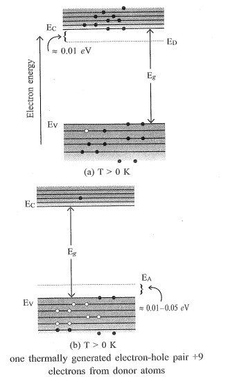
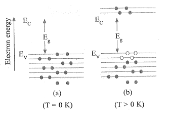
With no external energy, (at 0 K temperature), all the valence electrons will reside in the valence band.
• Energy band in the case of the metallic conductors :
If the lowest level in the conduction band happens to be lower than the highest level of the valence band (or when the conduction band overlaps with valence band) the electrons from the valence band can easily move into the conduction band.
The electrons in the conduction band can move freely and take part in the phenomenon of conduction of electricity.
This is the case with the metallic conductors.
• Energy band in case of Insulators :
If there is some gap between the conduction band and the valence band, electrons in the valence band all remain bound.
No single electron can move to the conduction band, which means no free electrons are available in the conduction band.
Therefore electricity can not flow (/conduct) through such material, hence it makes it insulator.
But some of the electrons from the valence band may get external energy to cross the gap between the conduction band and the valence band. Then these electrons will move into the conduction band.
View full question & answer
Question 152 Marks
Explain that the nature of electron motion in a solid is very different from that in an isolated atom.
Answer
According to the Bohr atomic model, in an isolated atom, the energy of any of its electrons is decided by the orbit in which it revolves.
But when the atoms come together to form a solid, they are close to each other.
So the outer orbits of the electrons from neighbouring atoms would come very close or could even overlap.
This would make the nature of electron motion in a solid very different from that in an isolated atom.
View full question & answer
Question 162 Marks
Provide the classification of semi-conductors with example.
Answer
The Semi-conductors can be classified as follows:
(i) Elemental Semi-conductors : $S i$ and Ge
(ii) Compound Semi-conductors :
Example are :
(a) Inorganic : $C d S, G a A s, C d S e, I n P$ etc.
(b) Organic : anthracene, doped pthalocyanines, etc.
(c) Organic polymers : polypyrrole, polyaniline, polythiophene etc.
Most of the currently available semi-conductor devices are based on elemental semiconductors $S i$ or $G e$ and compound inorganic semiconductors.
View full question & answer
Question 172 Marks
Provide the classification of solids on the basis of the relative values of electrical conductivity $(\sigma)$ or resistivity $( \rho ).$
Answer
$\rightarrow$ On the basis of the relative values of electrical conductivity $(\sigma)$ or resistivity $\left(\rho=\frac{1}{\sigma}\right)$ the solids can be classified as follows:
$(i)$ Metals :
$\rightarrow$ They possess very low resistivity $($or high conductivity$).$
$\rho \sim 10^{-2} \text { to } 10^{-8} \Omega m$
$\sigma \sim 10^2 \text { to } 10^8 Sm ^{-1}$
$(ii)$ Semiconductor :
$\rightarrow$ They have resistivity or conductivity intermediate to metals and insulators.
$\rho \sim 10^{-5} \text { to } 10^6 \Omega m$
$\sigma \sim 10^5 \text { to } 10^{-6} Sm ^{-1}$
$(iii)$ Insulators :
$\rightarrow$ They have high resistivity $($or low conductivity$).$
$\rho \sim 10^{11} \text { to } 10^{19} \Omega m$
$\sigma \sim 10^{-11} \text { to } 10^{-19} Sm ^{-1}$
View full question & answer
Question 182 Marks
Write down the difference between vacuum tube (valve) and semiconductors.
Answer
 Vacuum tubeSemiconductor
1Devices and instruments made of vacuum tube are bulky in size.Devices/instruments made of semiconductor are comparatively small (compact) in size.
2They consume high power and operate at high voltages $(\sim 100 V$.)They consume low power and operate at low voltages.
3They have limited life and low reliability.They have long life and high reliability.
4Controlled flow of electrons is obtained by varying the voltage between its different electrodes.Controlled flow of electrons can be obtained by small applied voltage (or other simple excitations like light/ heat.)
View full question & answer
Question 192 Marks
Give brief explanation of modern solid state semi-conductor electronics.
Answer
The seed of the development of the modern solid-state semiconductor electronics goes back to 1930 's.
Then it was realized that some solid state semiconductors and their junctions offer the possibility of controlling the number and the direction of flow of charge carriers through them.
Simple excitations like light, heat or small applied voltage can change the number of mobile charges in a semiconductor, and hence can control the current. which means they act as a catalyst.
Note that the supply and flow of charge carriers in the semiconductor devices are within the solid itself.
Unlike the vacuum tubes/valves, no external heating or large evacuated space is required by the semi-conductor devices.
They are small in size, consume low power, operate at low voltages and have long life and high reliability.
Even the Cathode Ray Tubes (CRT) used in television and computer monitors which work on the principle of vacuum tubes are being replaced by Liquid Crystal Display (LCD) monitors with supporting solid state electronics.
Much before the full implications of the semiconductor devices were formally understood, a naturally occurring crystal of galena (lead sulphide, PbS ) with a metal point contact attached to it was used as a detector of radio waves.
View full question & answer
Question 202 Marks
Write a short note on 'Valves' in electronics.
Answer
Before the discovery of transistors in 1948, valves (vacuum tubes) were widely used in electronic circuits.
Types of valves are as follows:
(i) Vacuum diode : which has two electrodes Anode (often called plate), and cathode.
(ii) Vacuum triode : which has three electrodes - cathode, plate and grid.
(iii) Vacuum tetrode : which has anode, cathode and 2 grids, so total four electrodes.
(iv) Vacuum pentode : which has 5 electrodes.
In a vacuum tube, the electrons are supplied by a heated cathode (current is passed through the filament kept very close to the cathode and by heating the cathode, electrons are emitted by Thermionic emission process.)
Controlled flow of electrons in vacuum is obtained by varying the voltage between its different electrodes. Vacuum is required in the inter-electrode region (/space). Otherwise the moving electrons may lose their energy on collision with the air molecules in their path.
In these devices, the electrons can flow only from cathode to the anode (i.e. only in one direction). Therefore such devices are generally referred to as valves.
These vacuum tube devices are bulky, consume high power, operate generally at high voltages ( $\sim 100 V$ ) and have limited life and low reliability.
View full question & answer
Question 212 Marks
What are the basic building blocks of electronic circuits ? Mention their types.
Answer
Devices in which a controlled flow of electrons can be obtained are the basic building blocks of all the electronic circuits.
They are of two types :
(i) Vacuum tubes (also called valves)
(ii) Devices prepared from various types of semi-conductors used in the solid-state Semiconductor Electronics.
View full question & answer