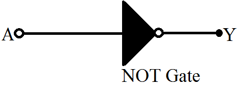
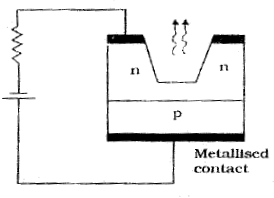
Question 13 Marks
Write the two processes that take place in the formation of a p-n junction. Explain with the help of a diagram, the formation of depletion region and barrier potential in a p-n junction.
Answer
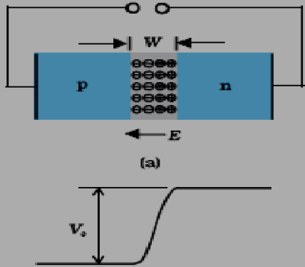
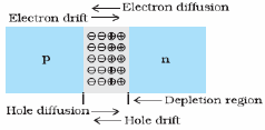
Due to the diffusion of electrons and holes across the junction a region of (immobile) positive charge is created on the n-side and a region of (immobile) negative charge is created on the p-side, near the junction; this is called depletion region.
Barrier potential is formed due to loss of electrons from n-region and gain of electrons by p-region. Its polarity is such that it opposes the movement of charge carriers across the junction.
View full question & answer→Due to the diffusion of electrons and holes across the junction a region of (immobile) positive charge is created on the n-side and a region of (immobile) negative charge is created on the p-side, near the junction; this is called depletion region.
Barrier potential is formed due to loss of electrons from n-region and gain of electrons by p-region. Its polarity is such that it opposes the movement of charge carriers across the junction.

 Principle


 Alternate Answer
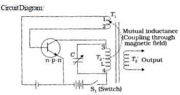
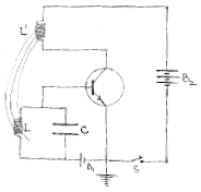 Explanation: By the process of mutual induction (or inductive coupling), energy is fedback to the tank circuit, in phase. The output in an oscillator is selfsustained.


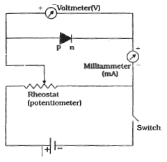
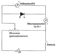
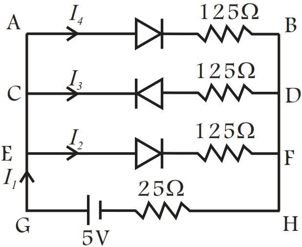
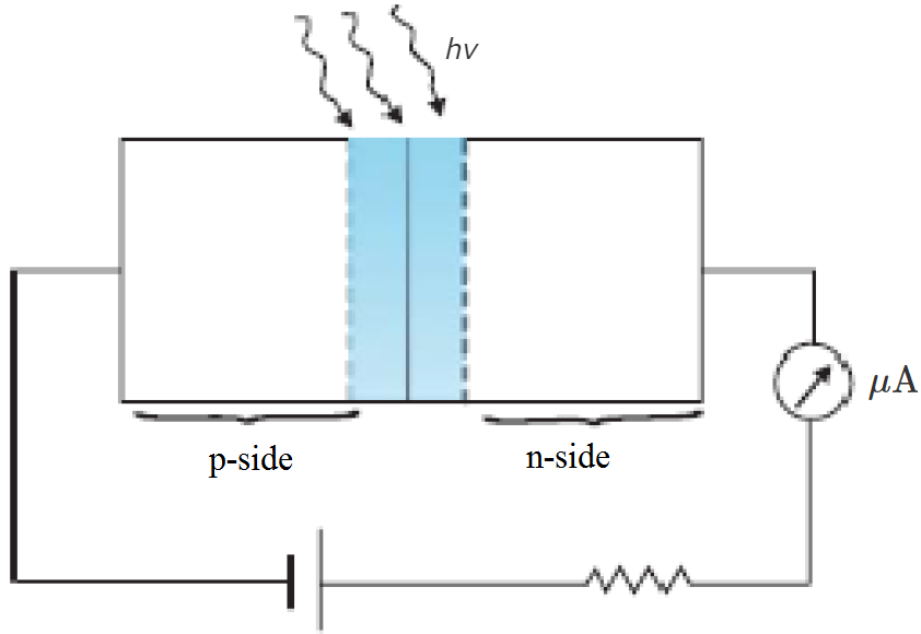
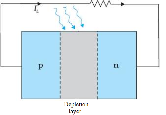
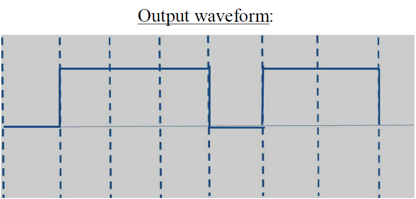
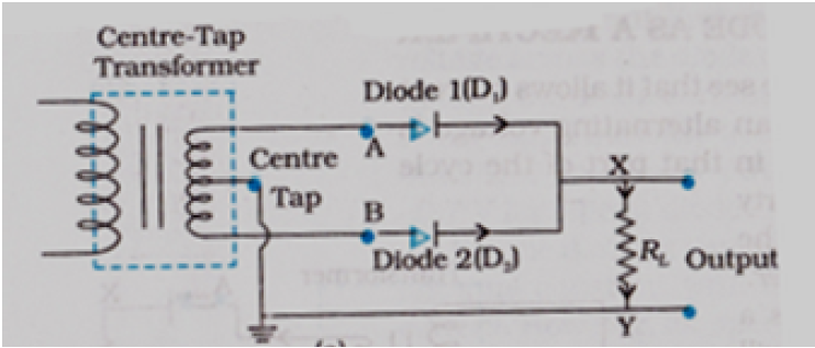
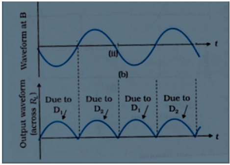
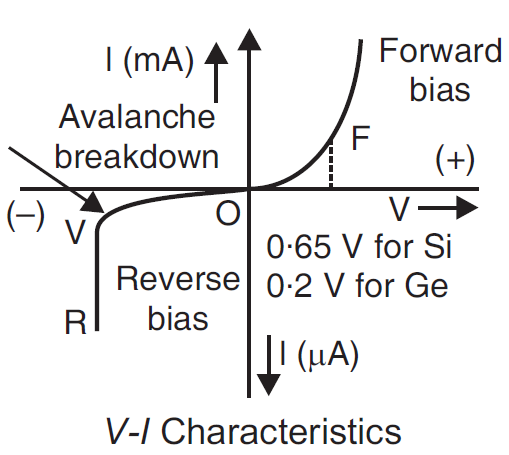
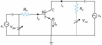
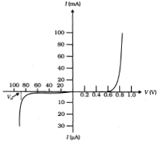
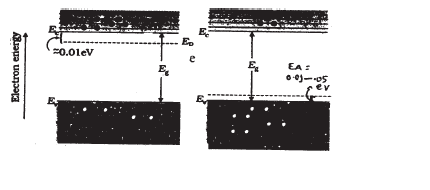
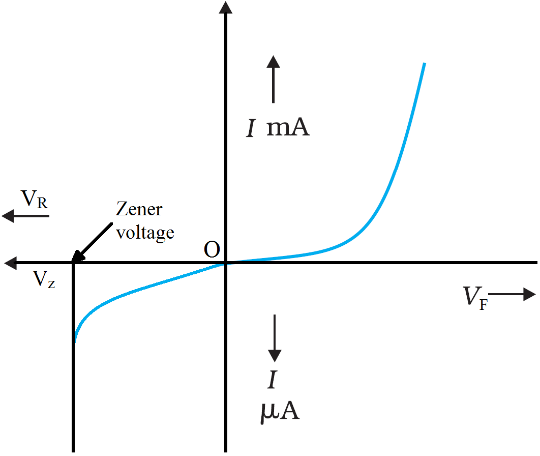
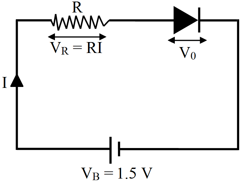
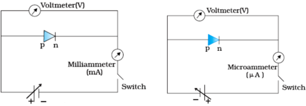 In forward bias, applied voltage does not support potential barrier. As a result, the depletion layer width decreases and barrier height is reduced. Due to the applied voltage, electrons from n side cross the depletion region and reach p side. Similarly holes from p side cross the junction and reach the n side. The motion of charged carriers, on either side, give rise to current. In reverse bias, applied voltage support potential barrier. As a result, barrier height is increased, depletion layer widens. This suppresses the flow of electrons from n → p and holes from p → n. Diffusion current decreases. The electric field direction of the junction is such that if electrons on p side or holes on n side in their random motion comes close to the junction, they will be swept to its majority zone. This drift of carriers give rise to the current called reverse current.
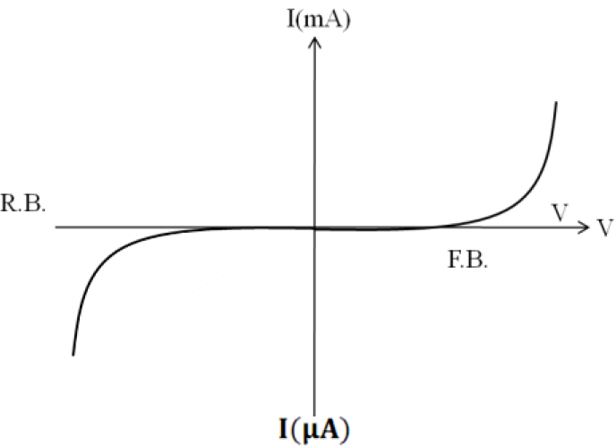
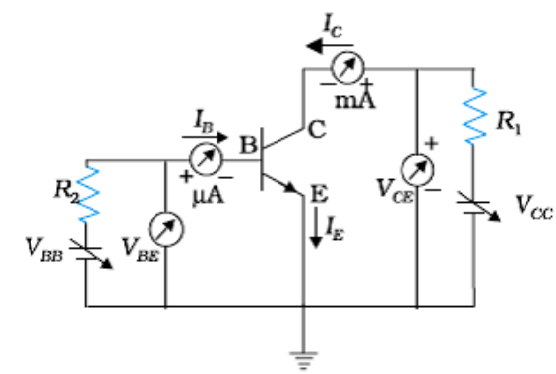
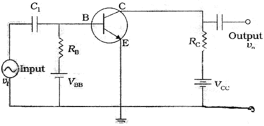
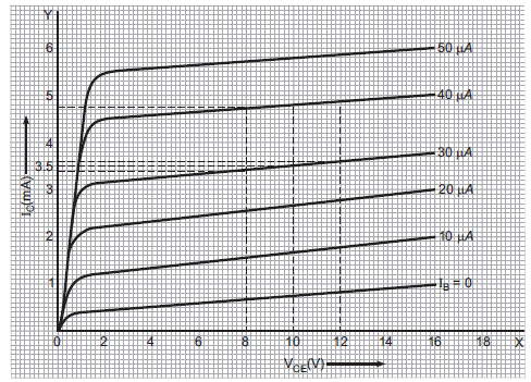
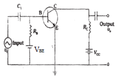
 Input resistance
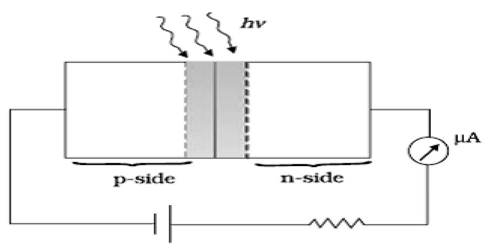
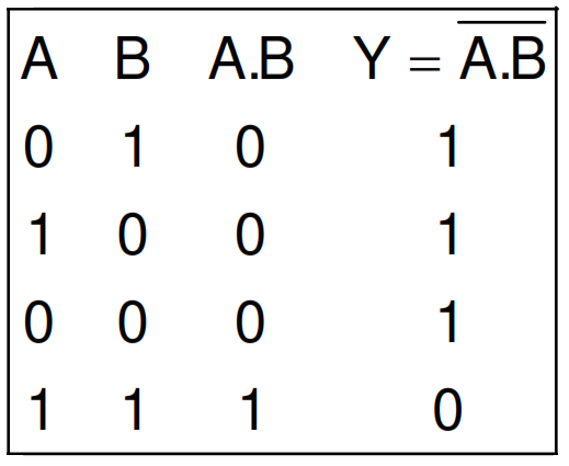
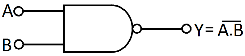
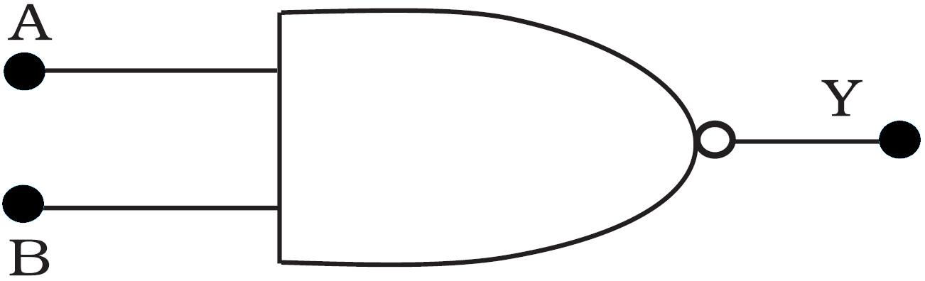
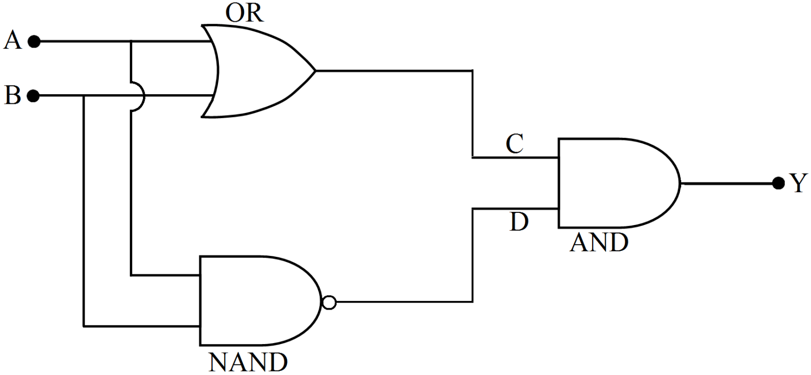
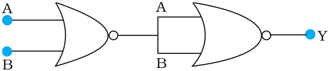
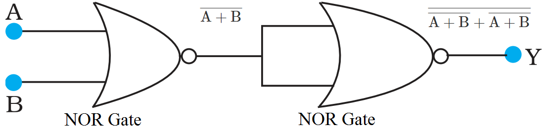
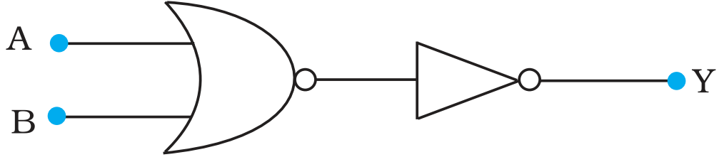
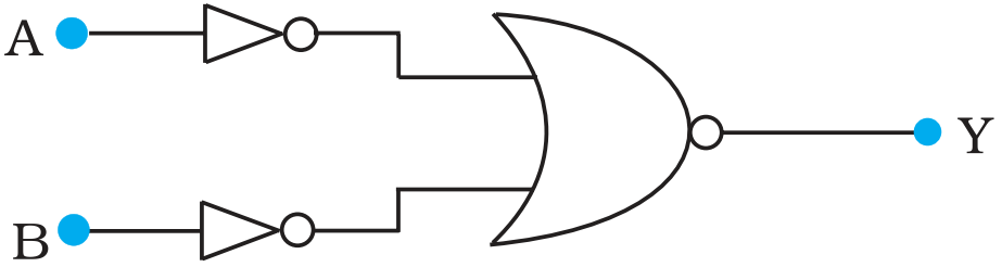
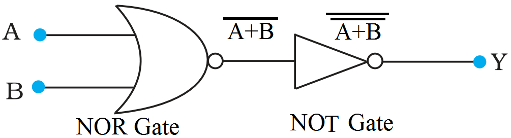
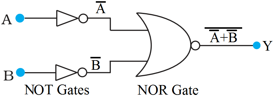
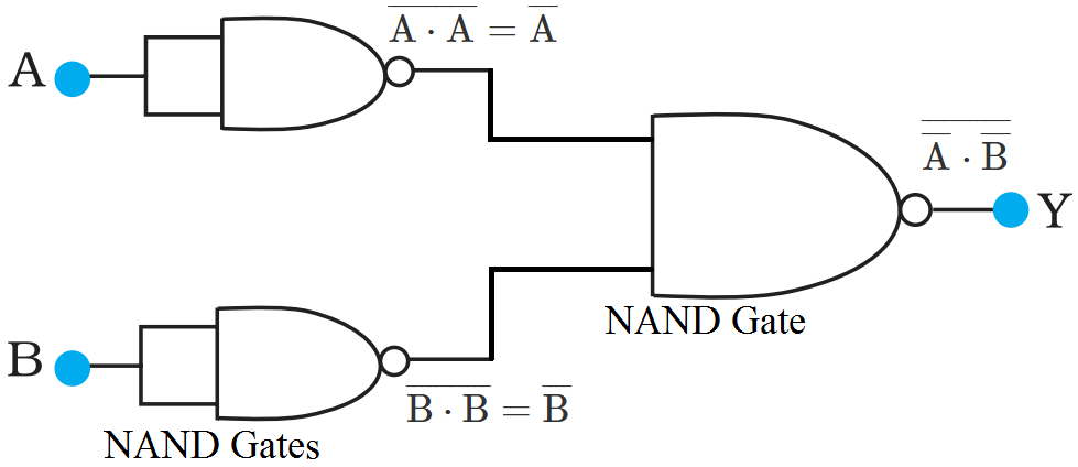
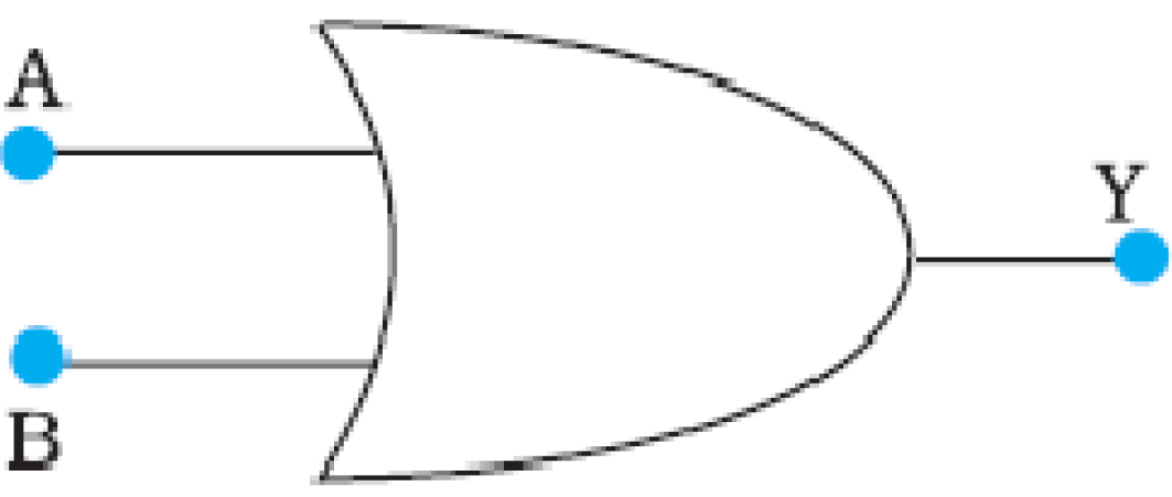
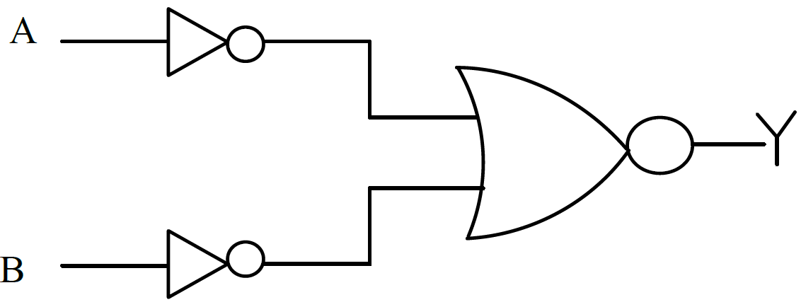
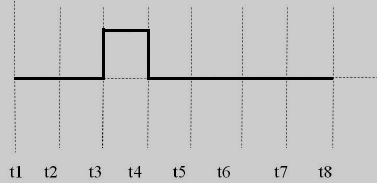
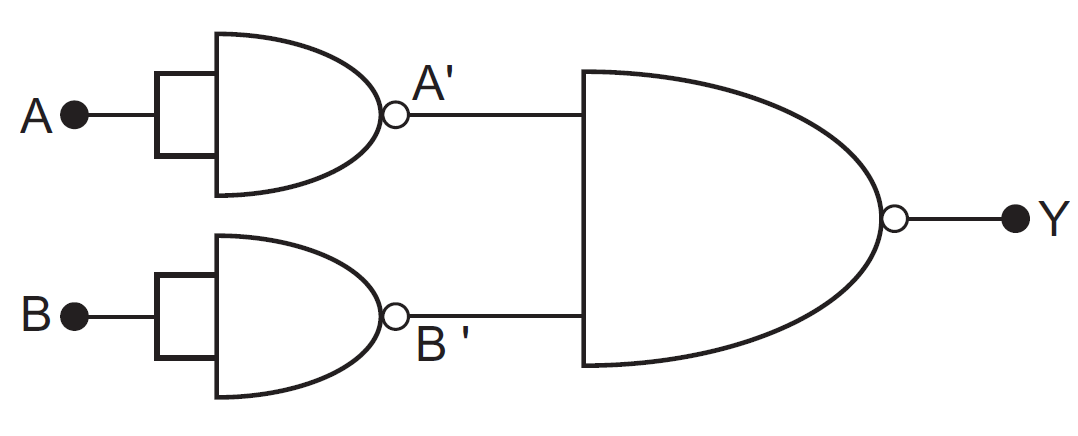
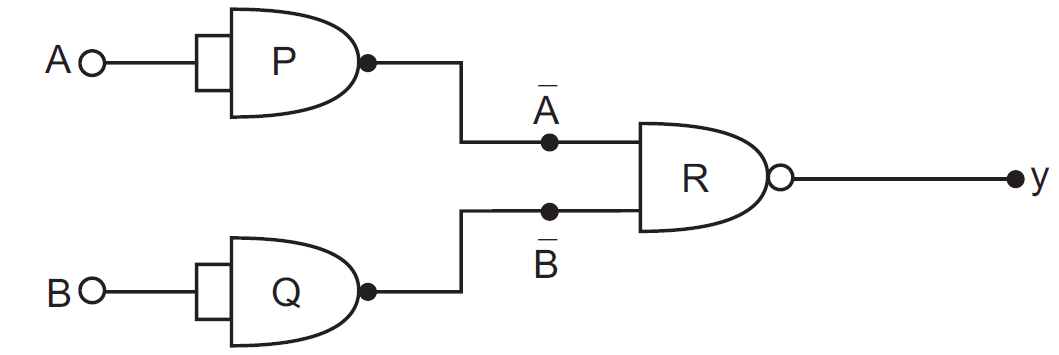
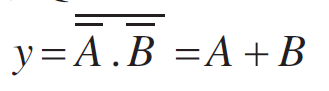
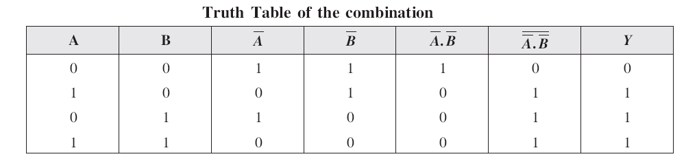
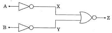
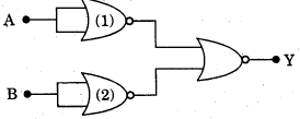
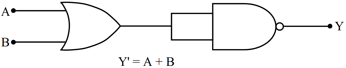 The logic circuit represents NOR gate.Its truth table is: