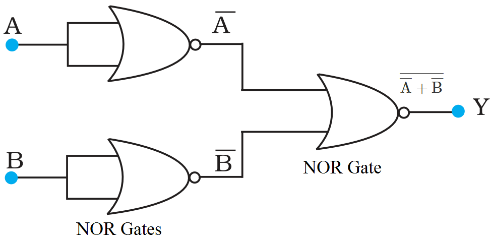
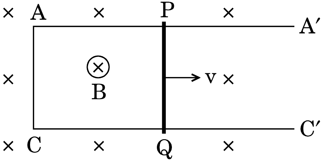
Questions

5 Marks Questions

Take a timed test

51 questions · self-marked practice — reveal the answer and mark yourself.

Question 15 Marks
In an intrinsic semiconductor the energy gap $E_{g}$ is $1.2eV$. Its hole mobility is much smaller than electron mobility and independent of temperature. What is the ratio between conductivity at $600K$ and that at $300K$? Assume that the temperature dependence of intrinsic carrier concentration $n_i$ is given by,
$\text{n}_{\text{i}}=\text{n}_{\text{0}}\ {\text{exp}}\Big(-\frac{\text{E}_\text{g}}{2{\text{K}_{\text{B}}}{\text{T}}}\Big)$
where $n_0$ is a constant.
Answer
Energy gap of the given intrinsic semiconductor $, E_g = 1.2 eV$
The temperature dependence of the intrinsic carrier $-$ concentration is written as: $\text{n}_{\text{i}}=\text{n}_{\text{0}}\ {\text{exp}}\Big[-\frac{\text{E}_\text{g}}{2{\text{K}_{\text{B}}}{\text{T}}}\Big]$
Where $, K_B =$ Boltzmann constant $= 8.62 \times 10^{-5} eV/K T$
$ =$ Temperature $n_0 =$ Constant Initial temperature $, T_1 = 300 K$
The intrinsic carrier $-$ concentration at this temperature can be written as: $\text{n}_{\text{i1}}=\text{n}_{\text{0}}\ {\text{exp}}\Big[-\frac{\text{E}_\text{g}}{2{\text{k}_{\text{B}}}\times300}\Big]...(1)$
Final temperature $, T_2 = 600 k$
The intrinsic carrier $-$ concentration at this temperature can be written as:
$\text{n}_{\text{i2}}=\text{n}_{\text{0}}\ {\text{exp}}\Big[-\frac{\text{E}_\text{g}}{2{\text{k}_{\text{B}}}\times600}\Big]...(2)$
The ratio between the conductivities at $600 K$ and at $300 K$ is equal to the ratio between the respective intrinsic carrier $-$ concentrations at these temperatures.
$\frac{\text{n}_{\text{i2}}}{\text{n}_{\text{i1}}}=\frac{\text{n}_\text{0}\ \text{exp}\Big[-\frac{\text{E}_{\text{g}}}{2\text{K}_{\text{B}}600}\Big]}{\text{n}_\text{0}\ \text{exp}\Big[-\frac{\text{E}_{\text{g}}}{2\text{K}_{\text{B}}300}\Big]}$
$=\text{exp}\frac{\text{E}_\text{g}}{2\text{k}_\text{g}}\bigg[\frac{1}{300}-\frac{1}{600}\bigg]$ $=\text{exp}\bigg[\frac{1.2}{2\times8.62\times10^{-5}}\times\frac{2-1}{600}\bigg] $
$= \text{exp} [11.6] = 1.09 \times 10^5$
Therefore, the ratio between the conductivities is $1.09 \times 10^5$.
View full question & answer
Question 25 Marks
In a $p-n$ junction diode, the current I can be expressed as,
$I=I_0\ \text{exp}\Big(\frac{\text{eV}}{2\text{k}_{\text{B}}\text{T}}-1\Big)$
where $I_0$ is called the reverse saturation current $, V$ is the voltage across the diode and is positive for forward bias and negative for reverse bias, and $I$ is the current through the diode $, k_g$ is the Boltzmann constant $(8.6\times 10^{-5} eV/K)$ and $T$ is the absolute temperature. If for a given diode $I_0 = 5\times 10^{-12} A$ and $T = 300 K,$ then,
  1. What will be the forward current at a forward voltage of $0.6V$?
  2. What will be the increase in the current if the voltage across the diode is increased to $0.7V$?
  3. What is the dynamic resistance?
  4. What will be the current if reverse bias voltage changes from $1V$ to $2V$?
Answer
In a $p-n$ junction diode, the expression for current is given as: $I=I_0\ \text{exp}\Big(\frac{\text{eV}}{2\text{k}_{\text{B}}\text{T}}-1\Big)$
Where, $I_0 =$ Reverse saturation current $= 5 \times 10^{-12} A T =$ Absolute temperature $= 300K k_B=$ Boltzmann constant $= 8.6 \times 10^{-5} eV/K = 1.376 \times 10^{-23} J K ^{-1} V =$ Voltage across the diode
  1. Forward voltage $, V = 0.6 V$
$\therefore\text{Current,}\ I=5\times10^{-12}\Bigg[\text{exp}\Bigg(\frac{1.6\times10^{-19}\times0.6}{1.376\times10^{-23}\times300}\Bigg)-1\Bigg]$
$= 5 \times 10^{-12} \times exp [22.36] = 0.0256 A$
Therefore, the forward current is about $0.0256 A$.
  1. For forward voltage $, V = 0.7 V,$ we can write:
$I=5\times10^{-12}\Bigg[\text{exp}\Bigg(\frac{1.6\times10^{-19}\times0.7}{1.376\times10^{-23}\times300}-1\Bigg)\Bigg]$
$= 5 \times 10^{-12} \times exp [26.25] = 1.257 A$
Hence, the increase in current, $\Delta{I}=I'-I$
$= 1.257 - 0.0256 = 1.23 A$
$\text{Dynamic resistance }=\frac{\text{Change in voltage}}{\text{Change in current}}$
  1. Dynamic resistance
$=\frac{0.7-0.6}{1.23}=\frac{0.1}{1.23}=0.081\Omega$
  1. If the reverse bias voltage changes from $1V$ to $2V,$ then the current $I$ will almost remain equal to $I_0$ in both cases.
  2. Therefore, the dynamic resistance in the reverse bias will be infinite.
View full question & answer
Question 35 Marks
Write the truth table for the circuits given in Fig. 14.48 consisting of NOR gates only. Identify the logic operations (OR, AND, NOT) performed by the two circuits.
  1.  
  1.  
Answer
  1. A acts as the two inputs of the NOR gate and Y is the output, as shown in the following figure. Hence, the output of the circuit is $\overline{{{\text{A}}}+{\text{A}}}.$

$\text{Output},\ \text{Y}=\overline{\text{A+A}}=\overline{\text{A}}$
The truth table for the same is given as:
A $_{\text{Y}}\Big(=\overline{\text{A}}\Big)$
0 1
1 0
This is the truth table of a NOT gate. Hence, this circuit functions as a NOT gate.
  1. A and B are the inputs and Y is the output of the given circuit. By using the result obtained in solution (a), we can infer that the outputs of the first two NOR gates are $\overline{\text{A}}\ \text{and}\ \overline{\text{B}},$ as shown in the following figure.

$\overline{\text{A}}\ \text{and}\ \overline{\text{B}},$ are the inputs for the last NOR gate. Hence, the output for the circuit can be written as:
$\text{Y} =\overline{\overline{\text{A}}+\overline{\text{B}}}=\overline{\overline{\text{A}}}\cdot\overline{{\overline{\text{B}}}}=\text{A}\cdot\text{B}$
The truth table for the same can be written as:
A B $\text{Y}(=\text{A}\Box\text{B})$
0 0 0
0 1 0
1 0 0
1 1 1
This is the truth table of an AND gate. Hence, this circuit functions as an AND gate.
View full question & answer
Question 45 Marks
  1. Describe briefly, with the help of a diagram, the role of the two important processes involved in the formation of a $p-n$ junction.
  2. Name the device which is used as a voltage regulator. Draw the necessary circuit diagram and explain its working.
Answer
  1.  

The two processes are:
  1. Diffusion.
  2. Drift.
Diffusion: Holes diffuse from $p –$ side to $n-$ side (p $\rightarrow$n) and electrons diffuse from $n–$ side to $p-$ side (n $\rightarrow$p)
Drift: The motion of charge carriers, due to the applied electric field$(\overrightarrow{\text{E}})$ which results in drifting of holes along$(\overrightarrow{\text{E}})$ and of electrons opposite to that of electric field$(\overrightarrow{\text{E}}).$
  1. Name of device: Zener Diode:

Working:
Any increase/decrease in the input voltage results in an increase/decrease of the voltage drop across $R_s$ without any change in voltage across the Zener diode. Thus Zener diode acts as voltage regulator.
View full question & answer
Question 55 Marks
  1. Draw the circuit diagrams of a $p-n$ junction diode in $(i)$ forward bias$, (ii)$ reverse bias. How are these circuits used to study the $V - I$ characteristics of a silicon diode? Draw the typical $V - I$ characteristics.
  2. What is a light emitting diode $\text{(LED)}$? Mention two important advantages of $\text{LEDs}$ over conventional lamps.
Answer


The battery is connected to the diode through a potentiometer $($or rheostat$)$ so that the applied voltage to the diode can be changed.
For different values of voltages, the value of the current is noted.
A graph between $V$ and $I$ is obtained.
Note that in forward bias measurement, we use a milliammeter $($since the expected current is large$)$ while a microammeter is used in reverse bias.

Typical $V-I$ characteristics of a silicon diode.
Light emitting diode:
It is a heavily doped $p-n$ junction which under forward bias emits spontaneous radiation.$/ p-n$ junction diode which emits light when forwardly biased.
Advantages:
  1. Low operational voltage and less power.
  2. Fast action and no warm$-$up time required.
  3. The bandwidth of emitted light is $100 \DeclareMathOperator*{\median}{\circ} \median_{\text{A}}$ to $500 \DeclareMathOperator*{\median}{\circ} \median_{\text{A}}$, or in other words it is nearly $($but not exactly$)$ monochromatic.
  4. Long life and ruggedness.
  5. Fast on$-$off switching capability.
View full question & answer
Question 65 Marks
  1. Draw the circuit arrangement for studying the input and output characteristics of an $n-p-n$ transistor in $CE$ configuration. With the help of these characteristics define $(i)$ input resistance $, (ii)$ current amplification factor.
  2. Describe briefly with the help of a circuit diagram how an $n-p-n$ transistor is used to produce self-sustained oscillations.
Answer
  1. Input resistance: This is defined as the ratio of change in base emitter voltage $(\triangle V_{BE} )$ to the resulting change in base current $(\triangle I_B )$ at constant collector $-$ emitter voltage $(V_{CE}).$
  2. $\text{r}_{1} = \bigg(\frac{\Delta\text{V}_{BE}}{\Delta\text{I}_{B}}\bigg)_{V_{CE}}$
  3. Current amplification factor (\beta): This is defined as the ratio of the change in collector current to the change in base current at a constant collector $-$ emitter voltage $(V_{CE})$ when the transistor is in active state.
  4. $\beta_{ac} = \bigg(\frac{\Delta\text{I}_{C}}{\Delta\text{I}_{B}}\bigg)_{V_{CE}}$
  5. Circuit diagram:

  6. Working: In an oscillator, we get an ac output without any external input signal.
  7. Hence, the output in an oscillator is self $-$ sustained.
  8. To attain this, an amplifier is taken. $A$ portion of the output power is returned back $($feedback$)$ to the input in phase with the starting power $($this process is termed positive feedback$).$
View full question & answer
Question 75 Marks
Explain the function of base region of a transistor. Why is this region made thin and lightly doped?  Draw a circuit diagram to study the input and output characteristics of n-p-n transistor in a common emitter (CE) configuration. Show these characteristics graphically. Explain how current amplification factor of the transistor is calculated using output characteristics.
Answer
Its acts as interface between emitter and collector. or It controls/regulates the charge carriers moving from emitter to collector. To minimise base current or ensuring that most of current carriers, moving out of the emitter,  move directly  from emitter to collector.


Current amplification factor: This is defined as the ratio of the change in collector current (output current) to the change in base current. $\beta = \bigg(\frac{\bigtriangleup\text{I}_{c}}{\bigtriangleup\text{I}_{B}}\bigg)_{\text{V}_{cb}}$.
View full question & answer
Question 85 Marks
What are energy bands? How are these formed? Distinguish between a conductor, an insulator and a semiconductor on the basis of energy band diagram.
Answer

A collection of closely spaced energy levels is called an energy band.
The energies of electrons in the outermost orbit may change due to the interaction between the electrons of different atoms. The 6 N states for $\ell =1 $, which originally had identical energies in the isolated atoms, spread out and form an energy band. At still smaller spacings, the energy bands again split apart and are separated by an energy gap Eg The total no. of available energy states 8N get re-apportioned between the two bands(4N states each in the lower and upper energy bands).


View full question & answer
Question 95 Marks
Sunil and his parents were travelling to their village in their car. On the way his mother noticed some grey coloured panels installed on the roof of a low building. She enquired from Sunil what those panels were and Sunil told his mother that those were solar panels.
  1. What were the values displayed by Sunil and his mother? State one value for each.
  2. In what way would the use of solar panels prove to be very useful?
  3. Name the semiconductor device used in solar panels. Briefly explain with the help of a diagram, how this device works.
Answer
  1. Value displayed by mother: Inquisitive/scientific temperament/wants to learn.
Value displayed by Sunil: Knowledgeable/helpful/considerate.
  1. Provide clean/green energy, Reduces dependence on fossil fuels, Environment friendly energy source.
  2. Solar Cell.
View full question & answer
Question 105 Marks
Gautam went for a vacation to the village where his grandmother lived. His grandmother took him to watch ‘nautanki’ one evening. They noticed a blackbox connected to the mike lying nearby. Gautam’s grandmother did not know what that box was. When she asked this question to Gautam, he explained to her that it was an amplifier.
  1. Which values were displayed by the grandmother? How can inculcation of these values in students be promoted?
  2. What is the function of an amplifier?
  3. Which basic electronic device is used in the amplifier?
Answer
  1. Inquisitive, loving, scientific temperament.
By encouraging students to ask questions.
By giving them tasks/projects and allowing students to use different media to find the solution to the given task,
  1. It is a device which produces an amplified copy of the signal.
  2. Transistor.
View full question & answer
Question 115 Marks
  1. Differentiate between three segments of a transistor on the basis of their size and level of doping.
  2. How is a transistor biased to be in active state?
  3. With the help of necessary circuit diagram, describe briefly how $n-p-n$ transistor in $CE$ configuration amplifies a small sinusoidal input voltage. Write the expression for the ac current gain.
Answer
  1. Emitter: It is of moderate size and heavily doped.
Base: It is very thin and lightly doped.
Collector: It is moderately doped and larger in size.
  1. Transistor is said to be in active state when its emitter $-$ base junction is $($suitably$)$ forward biased and base $-$ collector junction is $($suitably$)$ reverse biased.
  2.  

When a small sinusoidal voltage is superposed on the dc base bias, the base current will have sinusoidal variation superimposed on the value of $I_B$
As a consequence , the collector current also will have sinusoidal variations, superimposed on the value of $I_C ,$ producing corresponding (amplified)
changes in the value of $V_0.$
ac current gain $\beta_{ac} = \bigg(\frac{\Delta\text{I}_{c}}{\Delta\text{I}_{b}}\bigg)_{VCE}.$
View full question & answer
Question 125 Marks
Meeta’s father was driving her to the school. At the traffic signal, she noticed that each traffic light was made of many tiny lights instead of a single bulb. When Meeta asked this question to her father, he explained the reason for this. Answer the following questions based on above information:
  1. What were the values displayed by Meeta and her father?
  2. What answer did Meeta’s father give?
  3. What are the tiny lights in traffic signals called and how do these operate?
Answer
  1. Values displayed by Meeta: Inquisitive/ Keen Observer/ Scientific temperament/Values displayed by Father: Encouraging/Supportive.
  2. Meeta’s father explained that the traffic light is made up of tiny bulbs called light emitting diodes (LED).
  3. Light emitting diode These diodes (LED’s) operate under forward bias, due to which the majority charge carriers are sent from these majority zones to minority zones. Hence recombination occurs near the junction boundary, which releases energy in the form of photons of light.
View full question & answer
Question 135 Marks
  1. Draw the circuit diagram of a fullwave rectifier using $p-n$ junction diode. Explain its working and show the output, input waveforms.
  2. Show the output waveforms $(Y)$ for the following inputs $A$ and $B$ of
    1. $OR$ gate.
    2. $\ce{NAND}$ gate.
Answer

  1. Duringfirsthalf cycle:
    A is positive $\ce{w.r.t}$ centre tap but $B$ is negative, hence only diode $D_1$ conducts and current flows through the load in the sense $X$ to $Y$.
    During the second half cycle:
    B is positive $\ce{w.r.t}$ centre tap but $A$ is negative hence only diode $D_2$ conducts and again send currents through load from $X$ and $Y$.
    $\therefore$ Current through the load, in both the halves of input, is unidirectional.
  2.  
View full question & answer
Question 145 Marks
Draw a simple circuit of a $CE$ transistor amplifier. Explain its working. Show that the voltage gain $, A_V,$ of the amplifier is given by $\text{A}_{V} = - \frac{\beta_{ac}\text{R}_{L}}{\text{r}_{i}},$ where $ \beta_{ac}$ is the current gain $, R_L$ is the load resistance and $r_i$ is the input resistance of the transistor. What is the significance of the negative sign in the expression for the voltage gain?
Answer


When an ac input signal $v_i$ is superimposed on the bias $v_{BB},$ the output, which is measured between collector and ground, increases.
$\text{v}_{CC} = \text{v}_{CE} + \text{I}_{C}\text{R}_{L}$
$\text{v}_{BB} =\text{v}_{RE} + \text{I}_{B} \text{R}_{B}$
When $\text{v}_{i}$ is not zero, we have
$\text{v}_{BE} + \text{v}_{i} = \text{v}_{BE} + \text{I}_{B} \text{ R}_{B} +\Delta\text{I}_{B}(\text{R}_{B} + \text{R}_{i})$
$ \Rightarrow \text{v}_{i} = \Delta\text{I}_{B}(\text{R}_{B} + \text{R}_{i})$
$\text{v}_{i} =\text{r}\Delta\text{I}_{B}$
Change in $\text{I}_{B}$ causes a change in $\text{I}_{C}$
Hence, $\beta_{ac} = \frac{\Delta\text{I}_{C}}{\Delta\text{I}_{B}} =\frac{\text{I}_{C}}{\text{I}_{B}}$
As $\Delta\text{V}_{CC} = \Delta\text{V}_{CE} + \text{R}_{L}\Delta\text{I}_{C} = 0 $
$\Rightarrow \Delta\text{V}_{CE} = - \text{R}_{L}\Delta\text{I}_{C}$
$\Rightarrow \text{V}_{o} = -\text{R}_{L}\Delta\text{I}_{C}$
$\beta_{ac}\Delta\text{I}_{B}\text{R}_{L}$
$\Rightarrow $ voltage gain of the amplifier
$\text{A}_{V} =\frac{\text{V}_{o}}{\text{V}_{i}} =\frac{\Delta\text{V}_{CE}}{\text{r}\Delta\text{I}_{B}} = \frac{-\beta_{ac}\Delta\text{I}_{B}\text{R}_{L}}{\text{r}\Delta\text{I}_{B}}$
Negative sign in the expression shows that output voltage and input voltage have phase difference of $\pi$.
Alternate Answer
$($Also accept this derivation for voltage gain expression$)$
$\text{A}_{V}=\frac{\Delta\text{V}_{CE}}{\Delta\text{V}_{BE}} = \frac{-\Delta\text{I}_{C}\text{R}_{L}}{\Delta\text{I}_{B}\text{R}_{L}} $
But current gain
$\beta_{ac} = \frac{-\Delta\text{I}_{C}}{\Delta\text{I}_{B}}$
$ [=\text{A}_{v} = - \beta_{ac}\times\frac{\text{R}_{L}}{\text{R}_{L}}\bigg].$
View full question & answer
Question 155 Marks
  1. Explain the formation of depletion layer and potential barrier in a p-n junction.
  2. In the figure given below the input waveform is converted into the output waveform by a device ‘X’. Name the device and draw its circuit diagram.
  1. Identify the logic gate represented by the circuit as shown and write its truth table.
Answer
  1. Depletion region: Due to the concentration gradient across p-, and nsides, holes diffuse from p-side to n-side (p $\rightarrow$ n) and electrons diffuse from n-side to p-side (n$\rightarrow$p). As the electrons diffuse from n $\rightarrow$ p, a layer of positive charge (or positive space-charge region) is developed on n-side of the junction. Similarly as the holes diffuse, a layer of negative charge (or negative space-charge region) is developed on the p-side of the junction. This space-charge region on either side of the junction together is known as depletion region.
Barrier potential:
The loss of electrons from the n-region and the gain of electron by the pregion causes a difference of potential across the junction of the two regions. The polarity of this potential is such as. To oppose further flow of carriers.
  1. Full wave rectifier:
  1. AND Gate:
Input
Output
A
0
0
1
1
B
0
1
0
1
Y
0
0
0
1
View full question & answer
Question 165 Marks
  1. With the help of the circuit diagram explain the working principle of a transistor amplifier as an oscillator.
  2. Distinguish between a conductor, a semiconductor and an insulator on the basis of energy band diagrams.
Answer

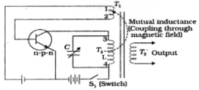
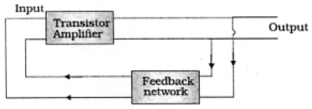
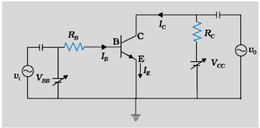
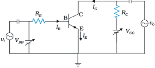
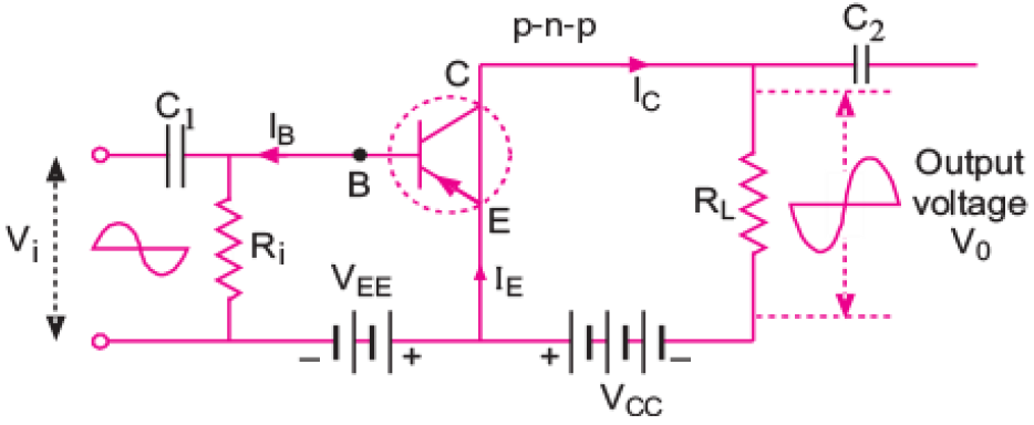
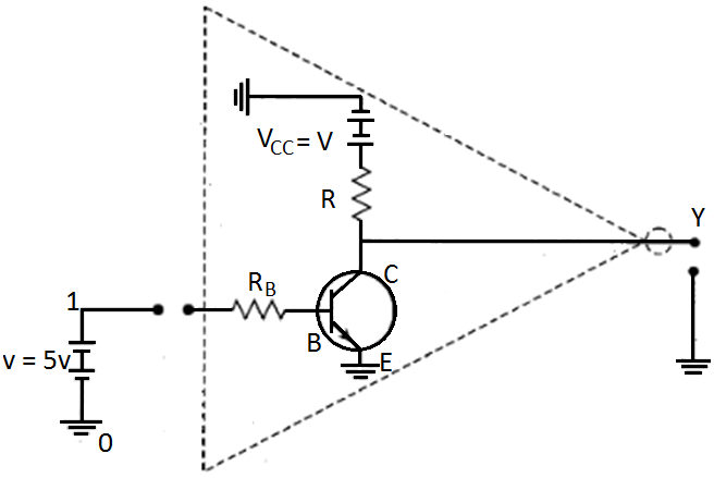
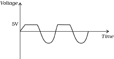
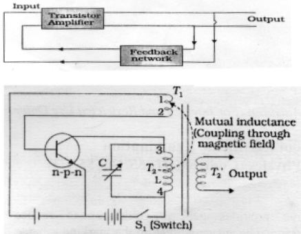
Working principle: In an oscillator, we get ac output without any external input signal, i.e. the output in an oscillator is self-sustained. To attain this, a portion of the output power of an amplifier, is returned back (fedback) to the input in phase with the starting power.
The energy band diagrams, showing the distinction between a conductor, a semiconductor and an insulator are shown below:
View full question & answer
Question 175 Marks
Draw the symbolic representation of a $(i)\ p-n-p, (ii)\ n-p-n$ transistor. Why is the base region of transistor thin and lightly doped? With proper circuit diagram, show the biasing of a $p-n-p$ transistor in common base configuration. Explain the movement of charge carriers through different parts of the transistor in such a configuration and show that $\text{I}_{E}= \text{I}_{C} =\text{I}_{B}$.
Answer
 
$(i)\ n-p-n$ transistor $(ii)\ p-n-p$ transistor
Base region is thin and lightly doped so that the most of the charge carriers from the emitter are able to diffuse through base and go to the collector.
 

A large number of holes from p-type emitter region flow towards the base.
These constitute the current through the emitter $I_{e.}$
These holes have a tendency to combine with the electrons in the $'n\ '$ region of the base.
Only a few holes $($less than $5\%)$ are able to combine with the electrons in the base region constituting base current $'I_b\ '$. Remaining $95\%$ of the holes, due to favourable negative potential at the collector move towards the collector region, and constitute collector current $'Ic\ '.$
$\therefore\text{I}_{e} = \text{I}_{b} + \text{I}_{c}.$
View full question & answer
Question 185 Marks
State the principle of working of p-n diode as a rectifier. Explain, with the help of a circuit diagram, the use of p-n diode as a full wave rectifier. Draw a sketch of the input and output waveforms.
Answer

Principle: P-n function diode conducts when it is forward biased and doesn’t conduct when it is reverse biased.
 

Explanation:
Wave form:


View full question & answer
Question 195 Marks
  1. With the help of a labelled diagram, explain the working of a step $-$ up transformer. Give reasons to explain the following:
  1. Find:
  2. External force required to move the rod with uniform velocity $v = 10\ cm/ s,$
  3. A conducting rod $PQ$ of length $20\ cm$ and resistance $0.1\Omega$ rests on two smooth parallel rails of negligible resistance $AA\ '$ and $CC\ '.$ It can slide on the rails and the arrangement is positioned between the poles of a permanent magnet producing uniform magnetic field $B = 0.4T$. The rails, the rod and the magnetic field are in three mutually perpendicular directions as shown in the figure. If the ends $A$ and $C$ of the rails are short circuited,
  4. The core of the transformer is laminated.
  5. Thick copper wire is used in windings.
  6. Power required to do so.
Answer
  1.  

$AC$ voltage $v_1$ is applied at primary $P$ of transformer $($with turns $N_P)$.
By self induction, pot diff developed is,
$\text{e}_\text{p}=-\text{N}_\text{P}\frac{\text{d}\phi}{\text{dt}}=\text{v}_1$
Also, by mutual induction, pot diff developed in secondary $($turns $N_S)$
$\text{e}_\text{s}=-\text{N}_\text{S}\frac{d\phi}{\text{dt}}=\text{v}_0$ output $AC$ voltage,
Here, $\frac{\text{d}\phi}{\text{dt}}=$ time rate of charge of magnetic flux of each turn
$\therefore\frac{\text{e}_\text{s}}{\text{e}_\text{s}}=\frac{\text{N}_\text{S}}{\text{N}_\text{P}}=\frac{\text{v}_0}{\text{v}_1}$
  1. Core is laminated to block or minimize the paths of eddy currents to minimize heat loss against resistance of core.
  2. Thick copper wire is used in order to reduce the resistance of transformer coil to
    minimize heat loss.
  1. $\text{F}=\text{ilB}=\Big(\frac{\text{Blv}}{\text{R}}\Big)\text{lB}=\frac{\text{B}^2\text{l}^2\text{v}}{\text{R}}$
$=\frac{(0.4)^2\times(20\times10^{-2})\times(10\times10^{-2})}{0.1}$
$=640\times10^{-4+2+1}$
$=6.4\times10^{-3}\text{N}$
  1. Power $=\text{P}=\text{Fv}=\frac{\text{B}^2\text{l}^2\text{v}^2}{\text{R}}$
$=6.4\times10^{-3}\times10\times10^{-2}$
$=6.4\times10^{-4}\text{watt}.$
View full question & answer
Question 205 Marks
Two car garages have a common gate which needs to open automatically when a car enters either of the garages or cars enter both. Devise a circuit that resembles this situation using diodes for this situation.
Answer

As car enters in either of the garages or both, the common gate opened automatically.
This means that if any one input is high, output will high otherwise low. The device is shown like this:

So, OR gate gives the desired output.
A B Y = A + B
0 0 0
0 1 1
1 0 1
1 1 1
View full question & answer
Question 215 Marks
How would you set up a circuit to obtain $\text{NOT}$ gate using a transistor?
Answer
  1.  It has only one input and only one output.
  2. Boolean expression is $Y = Ᾱ $ and is read as $ " y$ equals not $A\ " $.Logical symbol of $\text{NOT}$ gate.
  1. Realization of $\text{NOT}$ gate: The transistor is so biased that the collector voltage $V_{CC} = V\ ($Voltage corresponding to $1$ state$).$
The resistors $R$ and $R_B$ are so chosen that if the input is low,
i.e. $0, $ the transistor is in the cut off and hence the voltage appearing at the output will be the same as applied $V = 5V$.
Hence $Y = V($or state $ I).$
If the input is high, the transistor current is in saturation and the net voltage at the output $Y$ is $0\ ($in state $0).$
  1. Truth table for not gate: 
$A$ $Y = Ᾱ$
$0$ $1$
$1$ $0$
View full question & answer
Question 225 Marks

Find the current through the battery circuits shown in figure.
Answer
Both diodes are forward biased. Thus the net diode resistance is 0.

$\text{i}=\frac{5}{\frac{10\times10}{10+10}}=\frac{5}{5}=1\text{A}$
One diode is forward biased and other is reverse biased.

$\text{i}=\frac{\text{V}}{\text{R}_\text{net}}=\frac{5}{10+0}=\frac{1}{2}=0.5\text{A}$
View full question & answer
Question 235 Marks

  1. Name the type of a diode whose characteristics are shown in Fig. (A) and Fig. (B).
  2. What does the point P in Fig. (A) represent?
  3. What does the points P and Q in Fig. (B) represent?
Answer
  1. Fig. (a) represents the characteristics of Zener diode and curve (b) is of solar cell.
  2. In fig. (a), point P represents Zener breakdown voltage.
  3. In fig. (b), the point Q represents zero voltage and negative current. Which means the light falling on solar cell with atleast minimum threshold frequency gives the current in opposite direction to that due to a battery connected to solar cell. But for the point Q the battery is short circuited. Hence it represents the short circuit current.
And the point Pin Fig. (b) represents some open circuit, voltage on solar cell with zero current through solar cell.
It means, there is a battery connected to a solar cell which gives rise to the equal and opposite current to that in solar cell by virtue of light falling on it.
View full question & answer
Question 245 Marks

Draw the current-voltage characteristics for the device shown in figure. between the terminals A and B.
Answer
  1. If a battery is connected between terminals A and B, with positive terminal connected to point A and negative terminal connected to point B, then the diode will get forward biassed by the applied voltage. So, the current voltage graph for this circuit will be the same as that of the characteristic curves of a forward-biassed diode.
  1. If a battery is connected between terminals A and B, with positive terminal connected to point A and negative terminal connected to point B, then the upper diode will get forward biassed and the lower diode will get reverse biassed by the applied voltage. So, this lower branch can be replaced by an open circuit; hence, the current flow through this branch will be zero. The current flows only through the upper diode, so the circuit on simplification will become identical to the circuit in part (a). Hence, the current voltage graph for this circuit will be the same as that of the characteristic curves of a forward-biassed diode.
View full question & answer
Question 255 Marks
An $\text{X-OR}$ gate has following truth table:
$A$ $B$ $Y$
$0$ $0$ $0$
$0$ $1$ $1$
$1$ $0$ $1$
$1$ $1$ $0$
It is represented by following logic relation
$\text{Y}=\bar{\text{A}}.\text{B}+\text{A}.\bar{\text{B}}$
Build this gate using $\ce{AND, OR}$ and $\text{NOT}$ gates.
Answer
$\ce{XOR}$ gate can be realized by the combination of two $\ce{NOT}$ gates, two $\ce{AND}$ gates and one $OR$ gate.
According to the problem, the logic relation for the . given truth table is,
$\text{Y}=\bar{\text{A}}.\text{B}+\text{A}.\bar{\text{B}}=\text{Y}_1+\text{Y}_2$
When $\text{Y}_1=\text{A}.\text{B}$  and $\text{Y}_2=\text{A}.\bar{\text{B}}$
$Y_1$ can be obtainced as output of $\ce{AND}$ gate $I$ for which one input is of $A$ through $\ce{NOT}$ gate and another input is of $B. Y_2$ can be obtained as output of $\ce{AND}$ gate $II$ for which one input is of $A$ and other input is of $B$ through $\ce{NOT}$ gate.
Now $Y$ can be obtained as output from OR gate, where $Y_1$ and $Y_2$ are inputs of $OR$ gate.
Thus, the logic circuit of this relation is given below.
View full question & answer
Question 265 Marks
Draw the output signals $C_1$ and $C_2$ in the given combination of gates $(Fig.).$
Answer


$A$ $B$ $C$ $D$ $E$ $F$ $G$ $H$ $I$ $C_1$
$0$ $0$ $0$ $0$ $1$ $1$ $1$ $0$ $0$ $1$
$1$ $0$ $1$ $0$ $0$ $1$ $0$ $1$ $1$ $0$
$0$ $1$ $0$ $1$ $1$ $0$ $0$ $1$ $1$ $0$
$1$ $1$ $1$ $1$ $0$ $0$ $0$ $1$ $1$ $0$

 
$A$ $B$ $C$ $D$ $E$ $F$ $G$ $C_2$
$0$ $0$ $0$ $0$ $1$ $1$ $1$ $0$
$1$ $0$ $1$ $0$ $0$ $1$ $1$ $0$
$0$ $1$ $0$ $1$ $1$ $0$ $1$ $0$
$1$ $1$ $1$ $1$ $0$ $0$ $0$ $1$
View full question & answer
Question 275 Marks

Find the currents through the resistances in the circuits shown in figure.
Answer
  1. Since both the diodes are forward biased net resistance = 0

$\text{i}=\frac{2\text{V}}{2\Omega}=1\text{A}$
  1. One of the diodes is forward biased and other is reverse biase.
Thus the resistance of one becomes $\infty.$

$\text{i}=\frac{2}{2+\infty}=0\text{A}$
Both are forward biased.
Thus the resistance is 0.

$\text{i}=\frac{2}{2}=1\text{A}.$
One is forward biased and other is reverse biased.
Thus the current passes through the forward biased diode.

$\therefore\text{i}=\frac{2}{2}=1\text{A}.$
View full question & answer
Question 285 Marks
Three photo diodes $D1, D2$ and $D3$ are made of semiconductors having band gaps of $2.5eV, 2eV$ and $3eV,$ respectively. Which ones will be able to detect light of wavelength $6000\mathring{\text{A}}$?
Answer
Key concept: In Photo diodes electron and hole pairs are created by junction photoelectric effect.
That is the covalent bonds are broken by the $EM$ radiations absorbed by the electron in the $V.B$.
These are used for detecting light signals.

According to the problem,
Wavelength of light $\lambda=6000\mathring{\text{A}}=6000\times10^{-10}\text{m}$
Energy of the light photon
$\text{E}=\frac{\text{hc}}{\lambda}=\frac{6.6\times10^{-34}\times3\times10^8}{6000\times10^{-10}\times1.6\times10^{-19}}\text{eV}=2.06\text{eV}$
The incident radiation which is detected by the photodiode $D_2$ because energy of incident radiation is greater than the band $-$ gap.
View full question & answer
Question 295 Marks
Input signals $A$ and $B$ are applied to the input terminals of the ‘dotted box’ set$-$up shown here. Let $Y$ be the final output signal from the box.
Draw the wave forms of the signals labelled as $C_1$ and $C_2$ within the box, giving $($in brief$)$ the reasons for getting these wave forms. Hence draw the wave form of the final output signal $Y$. Give reasons for your choice.
What can we state $($in words$)$ as the relation between the final output signal $Y$ and the input signals $A$ and $B$?
Answer
$\text{C}_1=\bar{\text{A}}\cdot\text{B},\text{C}_2=\text{A}\cdot\bar{\text{B}}$
$\text{Y}=\text{C}_1\bar+\text{C}_2=\bar{\text{A}}\text{B}\bar+\bar{\text{B}}\text{A}$
This is Boolean expression for $\text{NOT XOR}$ gate.
$\text{C}_1=\bar{\text{A}}\cdot\text{B}$
 
$A$ $B$
$\text{C}_1=\bar{\text{A}}\cdot\text{B}$
From $0$ to $1$
$1$ $0$ $0$
From $1$ to $2$
$1$ $1$ $0$
From $2$ to $3$
$0$ $1$ $1$
From $3$ to $4$
$1$ $0$ $0$
From $4$ onwards
$1$ $0$ $0$

$\text{C}_2=\text{A}\cdot\bar{\text{B}}$
 
$A$ $B$
$\text{C}_2=\bar{\text{B}}\cdot{\text{A}}$
From $0$ to $1$
$1$ $0$ $1$
From $1$ to $2$
$1$ $1$ $0$
From $2$ to $3$
$0$ $1$ $0$
From $3$ to $4$
$1$ $0$ $1$
From $4$ onwards
$1$ $0$ $1$

$\text{Y}=\text{C}_1\bar+\text{C}_2$
 
$A$ $B$
$\text{Y}=\text{C}_1\bar+\text{C}_2$
From $0$ to $1$
$0$ $1$
$0$
From $1$ to $2$
$0$ $0$
$1$
From $2$ to $3$
$1$ $0$
$0$
From $3$ to $4$
$0$ $1$
$0$
From $4$ onwards
$0$ $1$
$0$

The gate shown in circuit is $\text{NOT XOR}$ gate.
According to definition the output $Y$ is obtained only if either both signals are $0$ or $1$. 
View full question & answer
Question 305 Marks
In the circuit shown in Fig., when the input voltage of the base resistance is $10V, V_{be}$ is zero and $Vce$ is also zero. Find the values of $I_b, I_c$ and $\beta.$
Answer
As $V_{BE} = 0,$ potential drop across $Rp$ is $10V.$
$\text{I}_\text{B}=\frac{\text{Voltage across R}_\text{B}}{\text{R}_\text{B}}=\frac{10}{400\times10^3}=25\times10^{-6}\text{A}=25\mu\text{A}$
Since, $\text{VCE} = 0$, potential drop across $R_c.$ i.e., $ I_cR_c$ is $10V.$
Voltage across $R_C = 10V$
$\text{I}_\text{C}=\frac{\text{Voltage across R}_\text{C}}{\text{R}_\text{C}}=\frac{10}{3\times10^3}=3.33\times10^{-3}\text{A}=3.33\mu\text{A}$
$\beta=\frac{\text{I}_\text{C}}{\text{I}_\text{B}}=\frac{3.33\times10^{-3}}{25\times10^{-6}}=1.33\times10^2=133$
View full question & answer
Question 315 Marks
The conduction band of a solid is partially filled at 0K. Will it be a conductor, a semiconductor or an insulator?
Answer
It will be a conductor. As the elements having partially filled conduction band belong to the category of elements whose outermost subshell consists of an odd number of electrons, they are good conductors of electricity. When an electric field is applied, electrons in the partially filled band gain energy and start drifting. So, the conductor will conduct even at 0K. A semiconductor behaves like an insulator at 0K and an insulator conducts poorly only at very high temperatures.
As the given material has free electrons to conduct even at 0K, it is a conductor.
View full question & answer
Question 325 Marks
The conductivity of an intrinsic samiconductor depends on temperature as $\sigma=\sigma_0\text{ e}^{\frac{-\Delta\text{E}}{2\text{kT}}}$ where $\sigma_0$ is a constant. Find the temperature at which the conductivity pf an intrinsic germanium semiconductor will be double of its value at T = 300K. Assume that the gap for germanium is 0.650eV and remains constant as the temperature is increased.
Answer
$\sigma=\sigma_0\text{e}^{\frac{-\Delta\text{E}}{2\text{KT}}}$
$\Delta\text{E}=0.650\text{eV},\text{T}=300\text{K}$
According to question, $\text{K}=8.62\times10^{-5}\text{eV}$
$\sigma_0\text{e}^{\frac{-\Delta\text{E}}{2\text{KT}}}=2\times\sigma_0\text{e}^{\frac{-\Delta\text{E}}{2\times\text{K}\times300}}$
$\Rightarrow\text{e}^{\frac{-0.65}{2\times8.62\times10^{-5}\times\text{T}}}=6.96561\times10^{-5}$
Taking in on both sides,
We get, $\frac{-0.65}{2\times8.62\times10^{-5}\times\text{T}'}=-11.874525$
$\rightarrow\frac{1}{\text{T}'}=\frac{11.574525\times2\times8.62\times10^{-5}}{0.65}$
$\Rightarrow\text{T}'=317.51178=318\text{K}.$
View full question & answer
Question 335 Marks
Explain why elemental semiconductor cannot be used to make visible LEDs.
Answer
Specially designed diodes, which give out light rediations when forward biases. LED's are made of GaAsp, Gap etc.
There are forwad biased P-N junctions which emits spontaneous fadiation. In elemental semiconductor, the band gap is such that the emission are in infrared region and not in visible region. $\lambda=\frac{\text{hc}}{\text{E}_\text{g}}$ For Si; $\text{E}_\text{g}= 1.1\text{eV},\lambda=\frac{1242}{1.1}=1129\text{nm}$ For Ge; $\text{E}_\text{g}=0.7\text{eV},\lambda=\frac{1242}{0.7}=1725\text{nm}$
View full question & answer
Question 345 Marks
How many is energy states are present in one mole of sodium vapour? Are they all filled in normal conditions? "How many $3s$ energy states are present in one mole of sodium vapour? Are they all filled in normal conditions?
Answer
For sodium, the atomic number is $11.$ The electronic configuration of sodium is $1s^{2 }2s^2 2p^6 3s^1.$ One sodium atom has $11$ electrons. Thus, if the sodium crystals consist of $N$ atoms, the total number of electrons will be $11N.$ We know that for each atom, there are two states in the energy level $1s.$ Thus, the sodium crystal will have $2N$ states for $1s$ energy level. Similarly, the number of states in $3s$ energy level will also be $2N. 1s$ state is filled under normal condition. But the $3s$ state has only one electron per sodium atom, so the $3s$ band will be half$-$filled.
View full question & answer
Question 355 Marks
If the resistance $R_1$ is increased $($Fig.$),$ how will the readings of the ammeter and voltmeter change?
Answer
Let us redrawn the circuit diagram to find the change in reading of ammeter and voltmeter.
So $, I_BR_1 + V_{BE} = V_{BB}$ Base current $, \text{I}_\text{B}=\frac{\text{V}_\text{BB}-\text{V}_\text{BE}}{\text{R}_1}$
$\text{I}_\text{B}\propto\frac{1}{\text{R}_1}$
So $, R_1$ is increased $, I_B$ is decreased.
Now, the current in ammeter is collector current $I_C. I_C = \beta\ I_B$ as $I_B$ is decreased $, I_C$ is also decreased and the reading of voltmeter and ammeter also decreased.
View full question & answer
Question 365 Marks
Assuming the ideal diode, draw the output waveform for the circuit given in Fig. Explain the waveform.
Answer
An ideal diode behaves like a perfect conductor when voltage is applied forward biased and like a perfect insulator when voltage is applied reverse biased.
When input voltage is greater than 5V, diode is conducting
When input is less than 5V, diode is open
The correct diagram is shown below:
View full question & answer
Question 375 Marks
The amplifiers $X, Y$ and $Z$ are connected in series. If the voltage gains of $X, Y$ and $Z$ are $10, 20$ and $30,$ respectively and the input signal is $1 mV$ peak value, then what is the output signal voltage (peak value):
  1. If $dc$ supply voltage is $10V$?
  2. If $dc$ supply voltage is $5V$?
Answer
Total voltage amplification is defined as the ratio of output signal voltage and input signal voltage.
According to the problem, voltage gain in $X, v_x = 10,$
voltage gain in $Y; v_y = 20,$
voltage gain in $Z, v_z = 30;$
$\Delta\text{V}_\text{i}=1\text{mV}=10^{-3}\text{V}$
and Total voltage amplification $= v_x \times v_y \times v_z$
$\Delta\text{V}_0=\text{v}_\text{x}\times\text{v}_\text{y}\times\text{v}_\text{z}\times\Delta\text{V}_\text{i}$
$= 10 \times 20 \times 30 \times 10^{-3} = 6V$
  1. If $DC$ supply voltage is $10V,$ then output is $6V,$ since theoretical gain is equal to practical gain, i.e., output can never be greater than $6V$.
  2. If $DC$ supply vpltage is $5V,$ i.e.$, V_{ce} = \%V. $
  3. Then, output peak will not exced $5V$.
  4. Hence $V_0 = 5V.$
View full question & answer
Question 385 Marks
In a CE transistor amplifier there is a current and voltage gain associated with the circuit. In other words there is a power gain. Considering power a measure of energy, does the circuit voilate conservation of energy?
Answer
Key concept: Different gain in CE transistor amplifier:
  1. Ac current gain: $\beta_\text{ac}=\Big(\frac{\Delta\text{i}_\text{c}}{\Delta\text{i}_\text{b}}\Big)\text{V}_\text{CE}=\text{constant}$
  2. dc current gain: $\beta_\text{dc}=\frac{\text{i}_\text{c}}{\text{i}_\text{b}}$
  3. Voltage gain: $\text{A}_\text{v}=\frac{\Delta\text{V}_0}{\Delta\text{V}_\text{i}}=\beta_\text{ac}\times\text{Resistance gain}$
  4. Power gain: $=\frac{\Delta\text{P}_0}{\Delta\text{P}_\text{i}}=\beta_\text{ac}^2\times\text{Resistance gain}$
The power gain is very high in CE transistor amplifier. In this circuit, the extra power required for amplified output is obtained from DC source. Thus, the circuit used does not violate the law of conservation.
View full question & answer
Question 395 Marks
When an electron goes from the valence band to the conduction band in silicon, its energy is increased by 1.1eV. The average energy exchanged in a thermal collision is of the order of kT which is only 0.026eV at room temperature. How is a thermal collision able to take some of the electrons from the valence band to the conduction band?
Answer
Fermi level: it is the energy level occupied by the highest energy electron.
In an extrinsic semiconductor for example in n-type semiconductor, fermi level lies close to the conduction band so it needs a very small amount of energy to excite the electron from fermi level to conduction band. This energy is comparable to the thermal excitation energy. So even at room temperature, these semiconductors can conduct. For a p-type semiconductor, fermi level lies close to valence bane because here conduction takes place majorly via holes. So by the thermal excitation, a bond is broken and an electron hole pair is created. Out of this, hole comes to the valence band for conduction or equivalently an electron goes to the conduction band. In an intrinsic semiconductor, no impurity is doped so fermi level lies at the centre of band gap. Here only few electrons get sufficient energy via repeated thermal collisions to jump from the fermi level to the conduction band. Hence the conductivity of intrinsic semiconductor is less as compared to extrinsic semiconductor.
View full question & answer
Question 405 Marks
Write the truth table for the circuit shown in Fig. Name the gate that the circuit resembles.
Answer
This is $'\text{AND}\ '$ Gate and its characteristics are as follows:
  1. It has tow inputs $(A$ and $B)$ and only one output $(Y).$
  1. Boolean expression is $Y = A.B$ is read as $"Y$ equals $\text{A AND B}".$
  2. Realization of $\text{AND}$ gate
  3.  
  1. $A = 0, B = 0$
  1. None of the diode conducts
    The out voltage ar $Y =$ Battery voltage $= 1$
  2. Truth table for $'\text{AND}"$ gate
  3. $D_1 =$ Conducts $, D_2 =$ Not conducts
    The out voltage at $Y =$ The voltage across the diode $(D_2) = 0$
  4. $A = 1, B = 1$
  5. $D_1 =$ Conducts $, D_2 =$ Not Conducts
    The out voltage at $Y = $ The voltage across the diode $(D_1) = 0$
  6. $A = 1, B = 1$
  7. The voltage supply throught $R$ is forward biasing diodes $D_1$ and $D_2 \ ($offers low resistance$),$ the voltage $V$ would drop across $R.$
    The output voltage at $Y =$ the voltage across diode $= 0.$
  8. $A = 0, B = 1$
$A$ $B$ $V_0 = A.B$
$0$ $0$ $0$
$0$ $1$ $0$
$1$ $0$ $0$
$1$ $1$ $1$
View full question & answer
Question 415 Marks
Consider a box with three terminals on top of it as shown in Fig (a): 
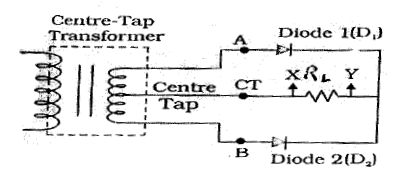
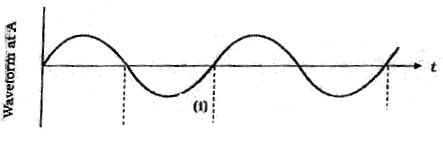
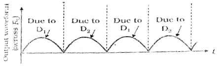
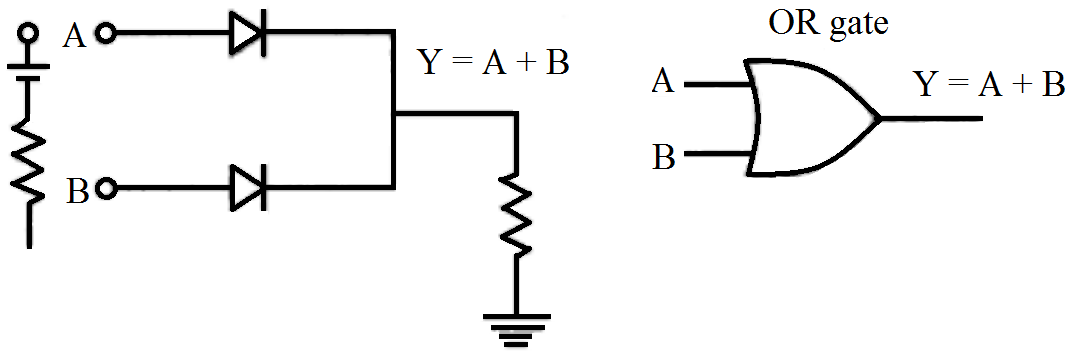
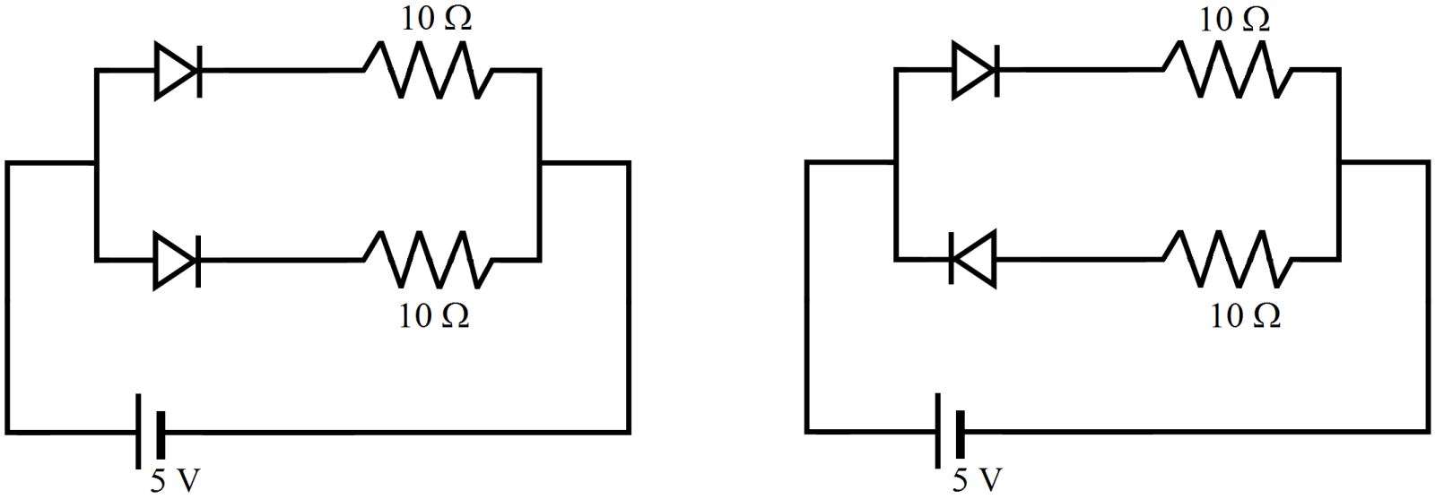
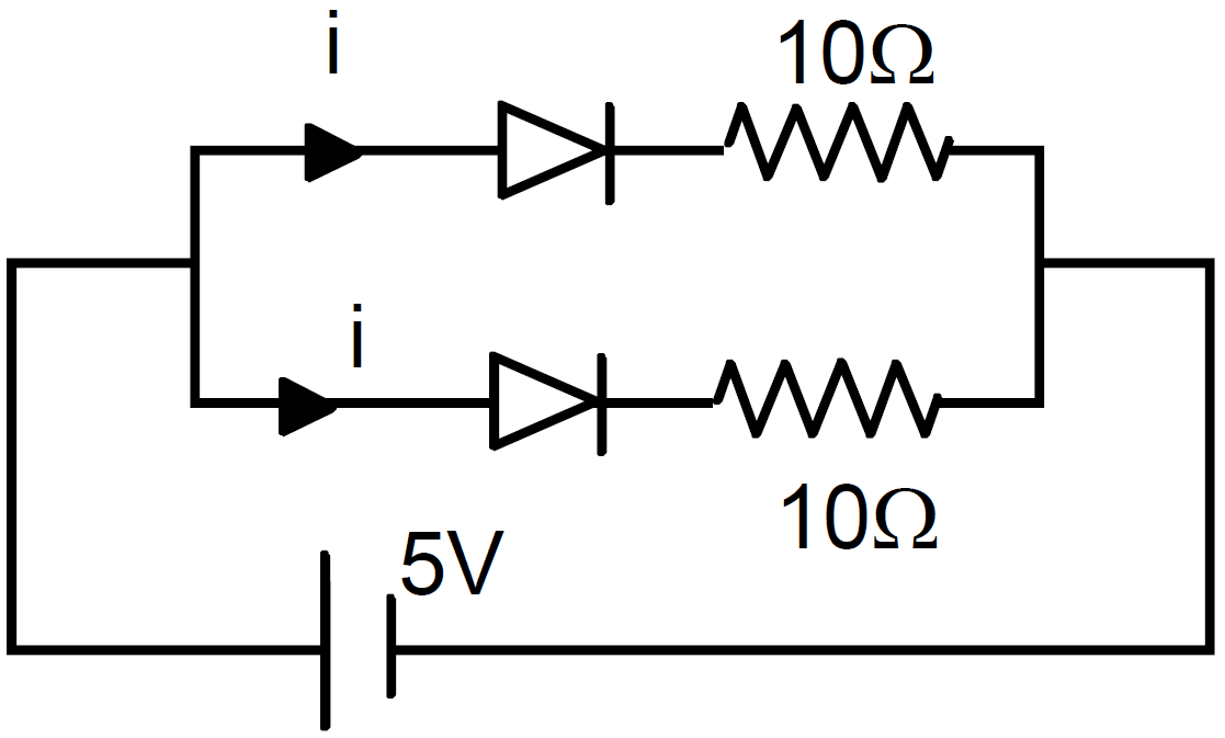
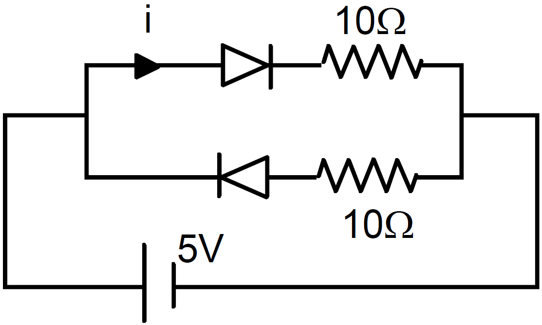
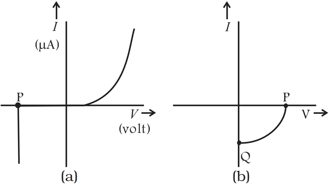
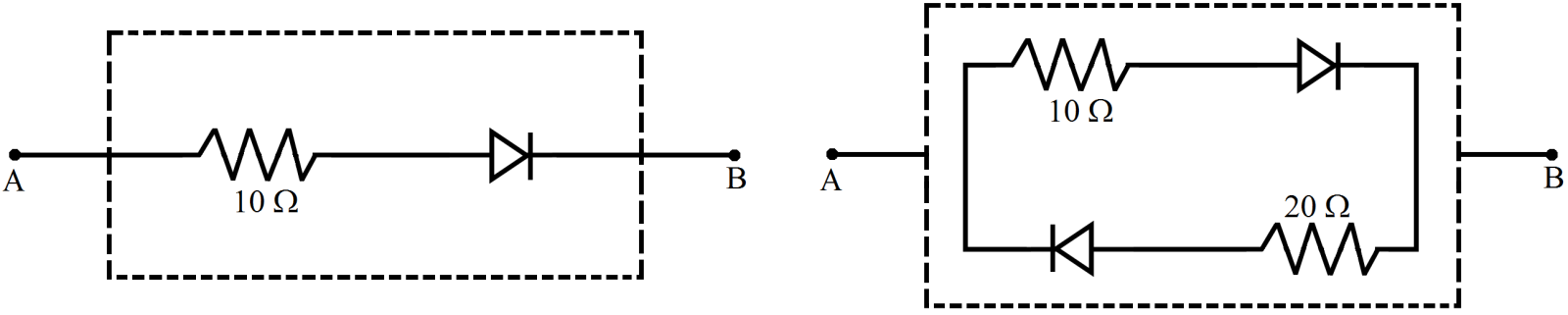
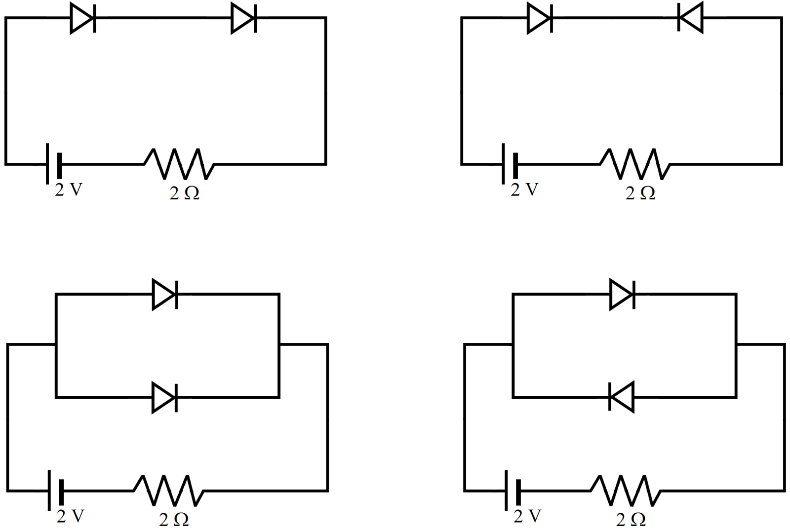
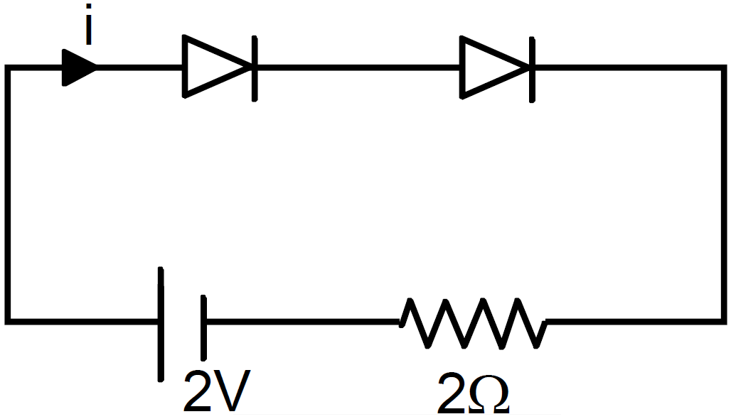
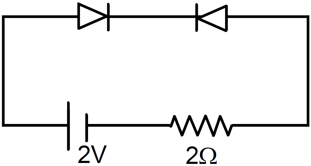
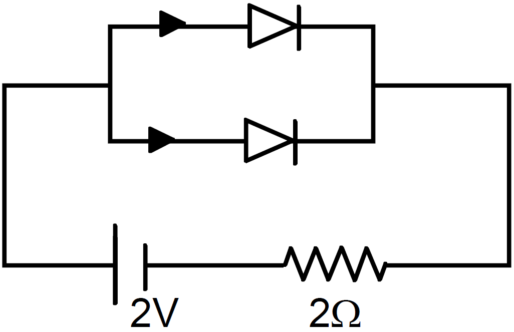
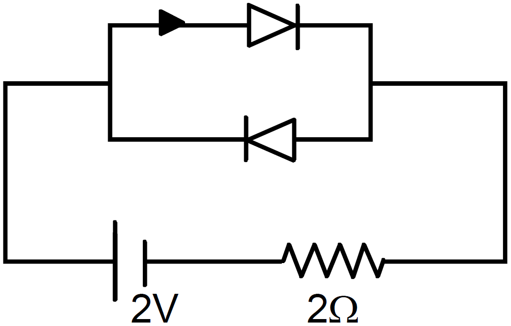
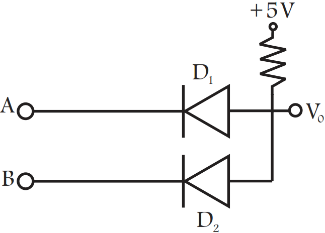
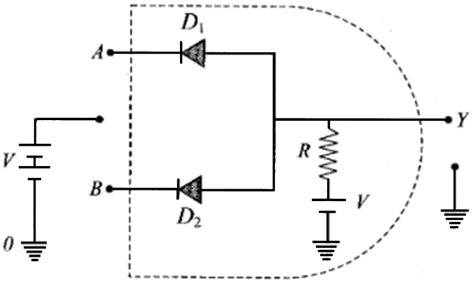
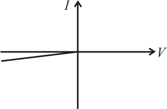
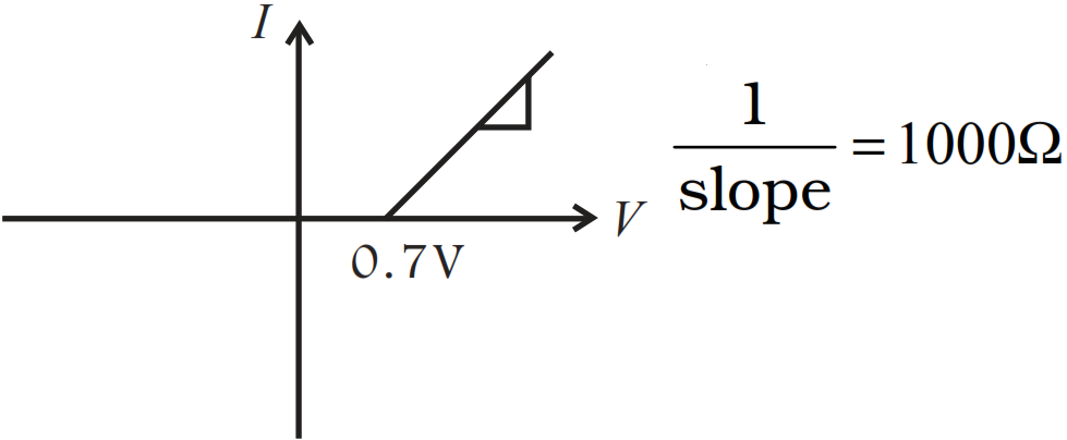
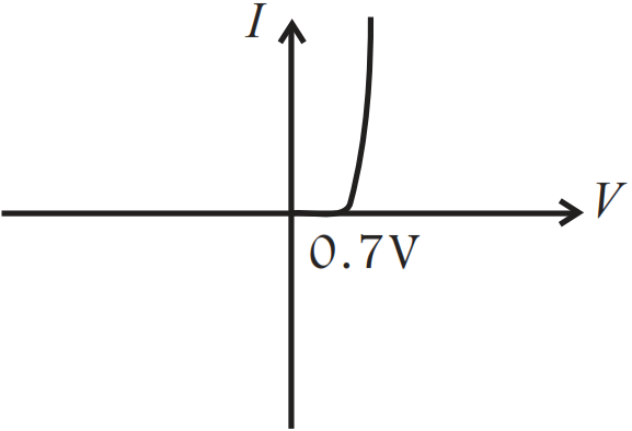
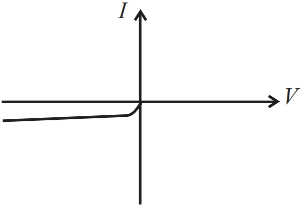
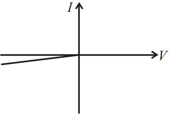
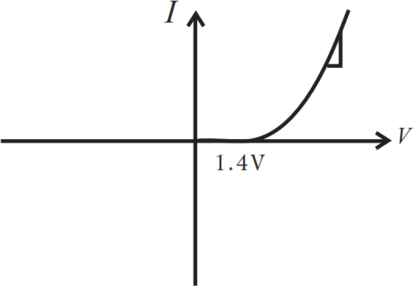
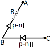
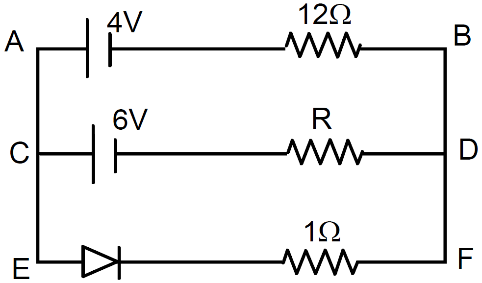
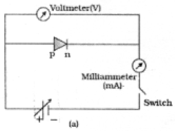
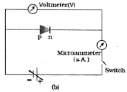
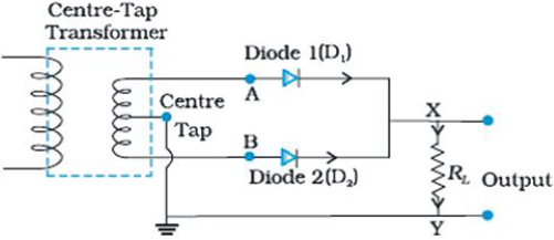
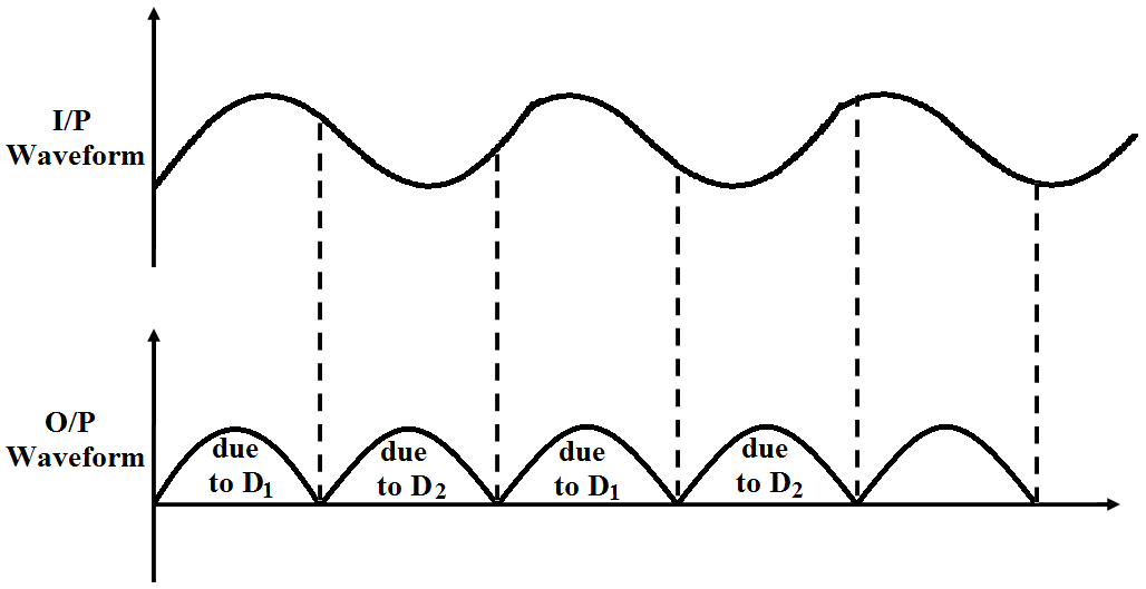
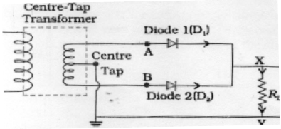
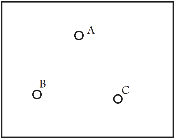
Three components namely, two germanium diodes and one resistor are connected across these three terminals in some arrangement. A student performs an experiment in which any two of these three terminals are connected in the circuit shown in Fig. (b). 
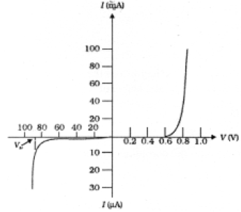
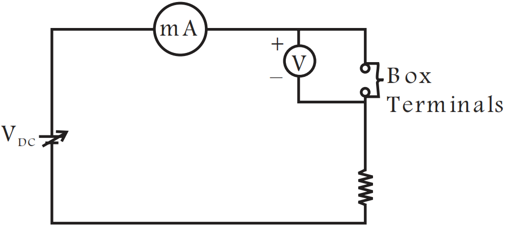
The student obtains graphs of current-voltage characteristics for unknown combination of components between the two terminals connected in the circuit. The graphs are
  1. When A is positive and B is negative,
  1. When A is negative and B is positive,
  1. When B is negative and C is positive,
  1. When B is positive and C is negative,
  1. When A is positive and C is negative,
  1. When A is negative and C is positive,

From these graphs of current - voltage characteristic shown in Fig. (c) to (h), determine the arrangement of components between A, B and C.
Answer
The V-I characteristics of these graph is discussed in points:
  1. In V-I graph of condition (i), a reverse characteristics is shown in fig. (c).
Here A is connected to n-side of p-n junction I and B is connected top-side of p-n junction I with a resistance in series.
  1. In V-I graph of condition (ii), a forward characteristics is shown in fig. (d), where 0.7 V is the knee voltage of p-n junction I. 1/slope = (1/1000)Ω.
It means A is connected to n-side of p-n junction I and B is connected to p-side of p-n junction I and resistance R is in series of p-n junction I between A and B.
  1. In V-I graph of condition (iii), a forward characteristics is shown in figure (e) , where 0.7 V is the knee voltage. In this case p-side of p-n junction II is connected to C and n-side of p-n junction II to B.
  2. In V-I graphs of conditions (iv), (v), (vi) also concludes the above connection of p-n junctions I and II along with a resistance R.
Thus, the arrangement of p-n I, p-n II and resistance R between A, B and C will be as shown in the figure.
View full question & answer
Question 425 Marks
In semiconductors, thermal collisions are responsible for taking a valence electron to the conduction band. Why does the number of conduction electrons not go on increasing with time as thermal collisions conμnuously take place?
Answer
An electron jumps from the valence band to the conduction band only when it has gained sufficient energy. The thermal collisions sometimes do not provide sufficient energy to the electron to jump. Also, energy is lost in the form of heat because of the collision of the carriers with other charge carriers and atoms. Because of all these losses, only few electrons are left with sufficient energy to jump from the valence band to the conduction band. So, the population of electron in the conduction band does not keep on increasing with time.
View full question & answer
Question 435 Marks
Consider a p-n junction diode having the characteristic $\text{i}-\text{i}_0\Big(\text{e}^{\frac{\text{eV}}{\text{kT}}}-1\Big)$ where $\text{i}_0=20\mu\text{A}.$ The diode is operated at T = 300K.
  1. Find the current through the diode when a voltage of 300mV is applied across it in forward bias.
  2. At what voltage does the current double?
Answer
  1. $\text{i}_0=20\times10^{-6}\text{A},\ \text{T}=300\text{K, V}=300\text{mV}$
$\text{i}=\text{i}_0\text{e}^{\frac{\text{eV}}{\text{KT}}-1}$ $=20\times10^{-6}\Big(\text{e}^{\frac{100}{8.62}}-1\Big)=2.18\text{A}=2\text{A}.$
  1. $4=20\times10^{-6}\Big(\text{e}^{\frac{\text{V}}{8.62\times3\times10^{-2}}}-1\Big)$
$\Rightarrow\text{e}^{\frac{\text{V}\times10^3}{8.62\times3}}-1=\frac{4\times10^6}{20}$
$\Rightarrow\text{e}^{\frac{\text{V}\times10^3}{8.62\times3}}=200001\Rightarrow\frac{\text{V}\times10^{3}}{8.62\times3}=12.2060$
$\Rightarrow\text{V}=315\text{mV}=318\text{mV}.$
View full question & answer
Question 445 Marks
When a p-n junction is reverse-biased, the current becomes almost constant at $25\mu\text{A}.$ When it is forwardbiased at 200mV, a current of $75\mu\text{A}$ is obtained. Find the magnitude of diffusion current when the diode is,
  1. Unbiased.
  2. Reverse-biased at 200mV.
  3. Forward-biased at 200mV.
Answer
  1. $\text{i}_1=25\mu\text{A},\text{V}=200\text{mV},\text{i}_2=75\mu\text{A}$
When in unbiased condition drift current = diffusion current
$\therefore$ Diffusion current $=25\mu\text{A}.$
  1. On reverse biasing the diffusion current becomes ‘O’.
  2. On forward biasing the actual current be x.
x - Drift current = Forward biasing current
$\Rightarrow\text{x}-25\mu\text{A}=75\mu\text{A}$
$\Rightarrow\text{x}=(75+25)\mu\text{A}=100\mu\text{A}.$
View full question & answer
Question 455 Marks
Find the current through the resistance R in figure. if.
  1. $\text{R}=12\Omega$
  2. $\text{R}=48\Omega$
Answer

  1. When $\text{R}=12\Omega$
The wire EF becomes ineffective due to the net (-)ve voltage.
Hence, current through $\text{R}=\frac{10}{24}=0.4166=042\text{A}.$
  1. Similarly for $\text{R}=48\Omega$
$\text{i}=\frac{10}{(48+12)}=\frac{10}{60}=0.16\text{A}.$
View full question & answer
Question 465 Marks
Suppose $a 'n\ ' -$ type wafer is created by doping $Si$ crystal having $5 \times 10^{28} \text{atoms/m^3}$ with $1 \text{ppm}$ concentration of As. On the surface $200 \text{ppm}$ Boron is added to create $'P\ '$ region in this wafer. Considering $n_i = 1.5 \times 10^{16}m^{-3}$.
  1. Calculate the densities of the charge carriers in the $n\ p$ regions.
  2. Comment which charge carriers would contribute largely for the reverse saturation current when diode is reverse biased.
Answer
  1. In $'n\ '$ region the number of majority carriers electrons due to doping of As is given by,
  1. $\text{n}_\text{e}=\text{N}_\text{D}=\frac{1}{16^6}5\times10^{28}=5\times10^{22}\text{m}^3$
    The minority carriers $($hole$)$ in $n -$ type wafer is given by,
    $\text{n}_\text{h}=\frac{\text{n}_\text{i}^2}{\text{n}_\text{e}}=\frac{(1.5\times10^{16})}{5\times10^{22}}=0.45\times10^{10}\text{m}^3$
    After $B$ is implanted in $Si$ crystal $, p-$type wafer is created with number of holes given by,
    $\text{n}_\text{h}=\text{N}_\text{A}=\frac{200}{10^6}\times(5\times10^{28})=10\times10^{25}/\text{m}^3$
    Minority carriers $($electrons$)$ created in $p-$ type wafer is given by
    $\text{n}_\text{e}=\frac{\text{n}_\text{h}^2}{\text{n}_\text{h}}=\frac{(1.5\times10^{16})}{1\times10^{25}}=2.25\times10^{27}/\text{m}^3$
  2. When $p-n$ juction is reverse biased, the minority carrier holes of $n-$ resion wafer $(n^h = 0.45 \times 10^{10}/m^3)$ would contribute more to the reverse saturation current than minority carrier $e^- (n_e = 2.25 \times 10^7/m^3)$ of $p$ region wafer.
View full question & answer
Question 475 Marks
The current $−$ voltage characteristic of an ideal $p-n$ junction diode is given by $\text{i}=\text{i}_0\Big(\text{e}^{\frac{\text{eV}}{\text{kT}}}-1\Big)$ where, the drift current $i_0$ equals $10\mu\text{A}.$ Take the temperature $T$ to be $300K.$
  1. Find the voltage $V_0$ for which $\text{e}^{\frac{\text{eV}}{\text{KT}}}=100.$ One can neglect the term $1$ for voltages greater than this value.
  2. Find an expression for the dynamic resistance of the diode as a function of $V$ for $V > V_0$.
  3. Find the voltage for which the dynamic resistance is $0.2\Omega.$
​​​​​​​
Answer
  1. The current‒voltage relationship of a diode is given by $\text{i}=\text{i}_0\Big(\text{e}^{\frac{\text{eV}}{\text{kT}-1}}\Big)$
For a large value of voltage $, 1$ can be neglected.
$\text{i}\approx\text{i}_0\text{e}^{\frac{\text{eV}}{\text{KT}}}$
Again, we need to find the voltage at which
$\text{e}^{\frac{\text{eV}}{\text{KT}}}=100$
$\Rightarrow\frac{\text{eV}}{\text{kT}}=\text{In }100$
$\Rightarrow\text{V}=\frac{\text{In }100\times\text{kT}}{\text{e}}$
$\Rightarrow\text{V}=\frac{2.303\times\log\ 100\times8.62\times10^{-5}\times300}{\text{e}}$
$\Rightarrow\text{V}=0.12\text{V}$
  1. Given:
$\text{i}=\text{i}_0\Big(\text{e}^{\frac{\text{eV}}{\text{kT}-1}}\Big)\ ...(1)$
We know that the dynamic resistance of a diode is the rate of change of voltage $\text{w.r.t}$. current.
i.e. $\text{R}=\frac{\text{dV}}{\text{di}}$
As the exponential factor dominates the factor of $1,$ we can neglect this factor.
Now, on differentiating eq. $(1)\ \text{w.r.t}. V,$ we get,
$\frac{\text{di}}{\text{dV}}=\text{i}_0\frac{\text{e}}{\text{kT}}\text{e}^{\frac{\text{eV}}{\text{kT}}}$
$\Rightarrow\frac{1}{\text{R}}=\frac{\text{ei}_0}{\text{kT}}\text{e}^{\frac{\text{eV}}{\text{kT}}}$
$\Rightarrow\text{R}=\frac{\text{kT}}{\text{ei}_0}\text{e}^{\frac{-\text{eV}}{\text{kT}}}\ ...(2)$
  1. Given,
$\text{R}=2\Omega$
On substituting this value in eq. $(2),$ we get
$2=\frac{8.62\times10^{-5}\times300}{\text{e}\times10\times10^{-6}}\text{e}^{\frac{\text{-eV}}{8.62\times10^{-5}\times300}}$
$\Rightarrow\text{V}=0.25\text{V}.$
View full question & answer
Question 485 Marks
In fig., the circuit symbol of a logic gate and two input waveforms A and B are shown:
  1. Name the logic gate.
  2. Write its truth table.
  3. Give the output waveform.
Answer
  1. The logic gate shown is OR gate.
  2. Truth table of OR gate is,
A
B
Y
0
0
0
1
0
0
0
1
0
1
1
1
  1. The input waveforms A and B are discrete square waves. The components of waveforms A and B are shown by vertical dotted lines.

Between a and b, A = 1, B = 1 → Y =1
Between b and c, A = 0, B = 0 → Y = 0
Between c and d, A = 0, B = 1 → Y = 1
Between d and e, A =1, B = 0 → Y = 1
Between e and f, A = 1, B = 1 → Y = 1
Between f and g, A = 0, B = 0 → Y = 0
Between g and h, A = 0, B = 1 → Y = 1
Accordingly, the waveform Y is shown as above.
View full question & answer
Question 495 Marks
Draw a labelled circuit diagram of a common emitter amplifier using a p-n-p transistor. Define the term voltage gain and write an expression for it. Explain how the input and output voltages are out of phase by 180° for a common-emitter transistor amplifiers.
Answer

Common-Emitter Transistor Amplifier: Given below is the circuit for a p-n-p transistor. In this circuit, the emitter is common to both the input (emitter-base) and output (collector-emitter) circuits and is grounded. The emitter-base circuit is forward biased and the base-collector circuit is reverse biased.
In a common-emitter circuit, the collector-current is controlled by the base-current rather than the emitter-current. Since in a transistor, when input signal is applied to base, a very small change in base-current provides a much larger change in collector-current and thus extremely large current gains are possible.

When positive half cycle is fed to the input circuit, it opposes the forward bias of the circuit which causes the collector current to decrease. It decreases the voltage drop across load RL and thus makes collector voltage more negative. Thus, when input cycle varies through a positive half cycle, the output voltage developed at the collector varies through a negative half cycle and vice versa. Thus, the output voltage in common-emitter amplifier is in antiphase with the input signal or the output and input voltages are 180° out of phase.
Current Gain. The ratio of change in collector current $(\Delta\text{I}_\text{C})$ to the change in base current $(\Delta\text{I}_\text{B})$ is called the alternating current gain denoted by $\beta$ Thus,
$\beta(\text{ac})=\frac{\Delta\text{I}_\text{C}}{\Delta\text{I}_\text{B}}$
$\beta$ has positive values and is generally greater than 20. Voltage Gain. The voltage gain of common- emitter transistor amplifier is given by,
$\text{A}_\text{v}=\frac{\Delta\text{V}_\text{out}}{\Delta\text{ V}_\text{in}}$
$=\frac{\text{R}_\text{L}\Delta\text{I}_\text{C}}{\text{R}_\text{i} \Delta\text{I}_\text{b}}$
$=\Big(\frac{\Delta\text{I}_\text{C}}{\Delta\text{I}_\text{b}}\Big)\cdot\frac{\text{R}_\text{L}}{\text{R}_\text{i}}$
$\Rightarrow\text{A}_\text{V}=\beta=\frac{\text{R}_\text{L}}{\text{R}_\text{i}}$
View full question & answer
Question 505 Marks

Identify which logic gate OR, AND and NOT is represented by the circuits in the dotted line boxes 1, 2 and 3. Give the truth table for the entire circuit for all possible values of A and B.
Answer
The dotted line box 1 represents NOT gate.
The dotted line box 2 represents OR gate.
The dotted line box 3 represents AND gate.
The output of box 1 is $\bar{\text{A}}$ The inputs of box 2 are A and ?̅
As box 2 is OR gate, therefore, output of box 2 is $\text{E}=(\bar{\text{A}}+\text{B}).$
The inputs of box 3 are E and B Box 3 represents AND gate; therefore, output of box 3 is,
$\text{Y}=\text{EB}=(\bar{\text{A}}+\text{B})\text{B}$
Truth table of the entire circuit is,
A
B
$\text{Y}=(\bar{\text{A}}+\text{B})\text{B}$
0
0
(1 + 0) . 0 = 0
1
0
(0 + 0) . 0 = 0
0
1
(1 + 1) . 1 = 1 . 1 = 1
1
1
(0 + 1) . 1 = 1 . 1 = 1
View full question & answer
Question 515 Marks
Consider the circuit arrangement shown in Fig $(a)$ for studying input and output characteristics of npn transistor in $CE$ configuration.

Select the values of $R_B$ and $R_C$ for a transistor whose $V_{BE} = 0.7V,$ so that the transistor is operating at point $Q$ as shown in the characteristics shown in Fig. $(b).$
Given that the input impedance of the transistor is very small and $V_{CC} = V_{BB} = 16V,$ also find the voltage gain and power gain of circuit making appropriate assumptions.
Answer
According to the problem, at point $Q,$ from graph $V_{BE} = 0.7V, V_{CC} = V_{BB} = 16V$ and $V_{CE} = 8V.$
$IC = 4mA = 4 \times 10^{-3}A$
$\text{I}_\text{B}=30\mu\text{A}=30\times10^{-6}\text{A}$
Since $, V_{CC} = I_CR_C + V_{CE}$
$\text{R}_\text{C}=\frac{\text{V}_\text{CC}-\text{V}_\text{CE}}{\text{I}_\text{C}}=\frac{16-8}{4\times10^{-3}}=\frac{8\times1000}{4}=2\text{k}\Omega$
Similarly $, V_{BB} - I_BR_B + V_{BE}$
$\text{R}_\text{B}=\frac{\text{V}_\text{BB}-\text{V}_\text{BE}}{\text{I}_\text{B}}=\frac{16-0.7}{30\times10^{-6}}$
$=510\times10^3\Omega=510\text{k}\Omega$
Current gain, $\beta=\frac{\text{I}_\text{C}}{\text{I}_\text{B}}=\frac{4\times10^{-3}}{30\times10^{-6}}=133.3$
Voltage gain $=\beta\frac{\text{R}_\text{C}}{\text{R}_\text{B}}=\frac{133\times2\times10^3}{510\times10^3}=0.52$
$\text{Power gain}=\beta\times\text{Voltage gain}=133\times0.52=69$
View full question & answer