MCQ 511 Mark
Resistance of semiconductor at $0^{\circ} K$ is
AnswerAt $0 K$ semiconductor behaves as insulator so it's resistance is infinite.
View full question & answer→MCQ 521 Mark
If $R_p=7 K \Omega, g_m=2.5$ millimho, then on increasing plate voltage by $50 V$, how much the grid voltage is changed so that plate current remains the same
- ✓
$-2.86\ V$
- B
$-4\ V$
- C
$+4\ V$
- D
$+2\ V$
AnswerCorrect option: A. $-2.86\ V$
$ \text { By using } \mu=-\frac{\Delta V_p}{\Delta V_g}=r_p \times g_m $
$ \Rightarrow 7 \times 10^3 \times 2.5 \times 10^{-3}=-\frac{50}{\Delta V_g}$
$ \Rightarrow \Delta V_g=-2.86 \mathrm{~V} .$
View full question & answer→MCQ 531 Mark
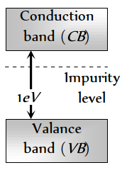
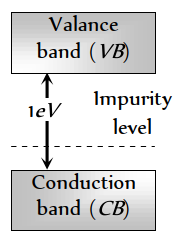
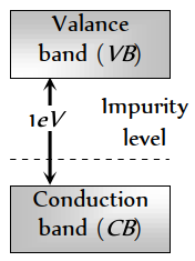
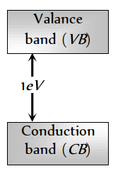
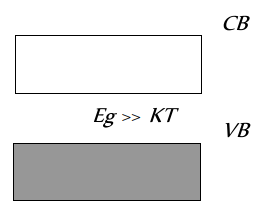
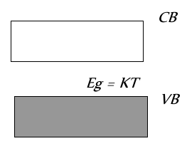
Which of the following energy band diagram shows the N-type semiconductor
AnswerIn $\mathrm{N}$-type semiconductor impurity energy level lies just below the conduction band.
View full question & answer→MCQ 541 Mark
Serious draw back of the semiconductor device is
- ✓
They cannot be used with high voltage
- B
They pollute the environment
- C
- D
They do not last for long time
AnswerCorrect option: A. They cannot be used with high voltage
View full question & answer→MCQ 551 Mark
Which of these is unipolar transistor
MCQ 561 Mark
In the $C B$ mode of a transistor, when the collector voltage is changed by $0.5$ volt. The collector current changes by $0.05\ mA$. The output resistance will be
- ✓
$10 \ k \Omega$
- B
$20\ k \Omega$
- C
$5\ k \Omega$
- D
$2.5 \ k \Omega$
AnswerCorrect option: A. $10 \ k \Omega$
Here $\Delta V_c=0.5 \mathrm{~V}, \Delta i_c=0.05 \mathrm{~mA}=0.05 \times 10 \mathrm{~A}$Output resistance is given by$R_{\text {out }}=\frac{\Delta V_c}{\Delta i_c}=\frac{0.5}{0.05 \times 10^{-3}}=10^4 \Omega=10 \mathrm{k} \Omega$
View full question & answer→MCQ 571 Mark
In case of a semiconductor, which of the following statement is wrong
- A
Doping increases conductivity
- B
Temperature coefficient of resistance is negative
- C
Resisitivity is in between that of a conductor and insulator
- ✓
At absolute zero temperature, it behaves like a conductor
AnswerCorrect option: D. At absolute zero temperature, it behaves like a conductor
At absolute zero temperature, semiconductor.
View full question & answer→MCQ 581 Mark
The relation between $\alpha$ and $\beta$ parameters of current gains for a transistors is given by
- A
$\alpha=\frac{\beta}{1-\beta}$
- ✓
$\alpha=\frac{\beta}{1+\beta}$
- C
$\alpha=\frac{1-\beta}{\beta}$
- D
$\alpha=\frac{1+\beta}{\beta}$
AnswerCorrect option: B. $\alpha=\frac{\beta}{1+\beta}$
$i_e=i_b+i_c \Rightarrow \frac{i_e}{i_c}=\frac{i_b}{i_c}+1$
$ \Rightarrow \frac{1}{\alpha}=\frac{1}{\beta}+1$
$ \Rightarrow\alpha=\frac{\beta}{(1+\beta)}$.
View full question & answer→MCQ 591 Mark
If $n$ and $v$ be the number of electrons and drift velocity in a semiconductor. When the temperature is increased
- ✓
$n$ increases and $v$ decreases
- B
$n$ decreases and $v$ increases
- C
Both $n$ and $v$ increases
- D
Both $n$ and $v$ decreases
AnswerCorrect option: A. $n$ increases and $v$ decreases
$n$ increases and $v$ decreases
View full question & answer→MCQ 601 Mark
For a transistor the parameter $\beta=99$. The value of the parameter $\alpha$ is
AnswerCorrect option: B. $0.99$
$\alpha=\frac{\beta}{1+\beta}=\frac{99}{1+99}=0.99$.
View full question & answer→MCQ 611 Mark
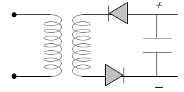
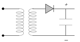
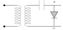
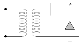
Which is the correct diagram of a half-wave rectifier
MCQ 621 Mark
In a transistor configuration $\beta$-parameter is
- A
$\frac{l_b}{l_c}$
- ✓
$\frac{l_c}{l_b}$
- C
$\frac{l_c}{l_a}$
- D
$\frac{l_a}{l_c}$
AnswerCorrect option: B. $\frac{l_c}{l_b}$
$\beta=\frac{i_c}{i_b}$
View full question & answer→MCQ 631 Mark
Doping of intrinsic semiconductor is done
- A
To neutralize charge carriers
- ✓
To increase the concentration of majority charge carriers
- C
To make it neutral before disposal
- D
To carry out further purification
AnswerCorrect option: B. To increase the concentration of majority charge carriers
View full question & answer→MCQ 641 Mark
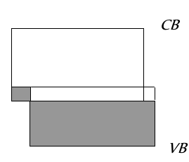
Which of the energy band diagrams shown in the figure corresponds to that of a semiconductor
AnswerIn semiconductors, the forbidden energy gap between the valence band and conduction band is very small, almost equal to $k T$. Moreover, valence band is completely filled where as conduction band is empty.
View full question & answer→MCQ 651 Mark
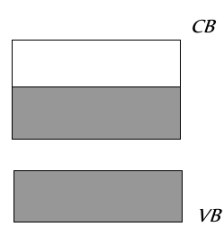
The valence band and conduction band of a solid overlap at low temperature, the solid may be
AnswerIn conductors valence band and conduction band overlaps.
View full question & answer→MCQ 661 Mark
If no external voltage is applied across $P-N$ junction, there would be
- A
No electric field across the junction
- ✓
An electric field pointing from $N$-type to $P$-type side across the junction
- C
An electric field pointing from $P$-type to $N$-type side across the junction
- D
A temporary electric field during formation of $P-N$ junction that would subsequently disappear
AnswerCorrect option: B. An electric field pointing from $N$-type to $P$-type side across the junction
Across the $P-N$ junction, a barrier potential is developed whose direction is from $N$ region to $P$ region.
View full question & answer→MCQ 671 Mark
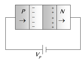
A semiconductor $X$ is made by doping a germanium crystal with arsenic $(Z=33)$. A second semiconductor $Y$ is made by doping germanium with indium $(Z=49)$. The two are joined end to end and connected to a battery as shown. Which of the following statements is correct
- A
(a) $X$ is $P$-type, $Y$ is $N$-type and the junction is forward biased
- B
(b) $X$ is $N$-type, $Y$ is $P$-type and the junction is forward biased
- C
(c) $X$ is $P$-type, $Y$ is $N$-type and the junction is reverse biased
- ✓
(d) $X$ is $N$-type, $Y$ is $P$-type and the junction is reverse biased
AnswerCorrect option: D. (d) $X$ is $N$-type, $Y$ is $P$-type and the junction is reverse biased
(d) Arsenic has five valence electrons, so it a donor impurity. Hence $X$ becomes $N$-type semiconductor. Indium has only three outer electrons, so it is an acceptor impurity. Hence $Y$ becomes $P$-type semiconductor. Also $N$ (i.e. $X$ ) is connected to positive terminal of battery and $P($ i.e. $Y)$ is connected to negative terminal of battery so $P N$-junction is reverse biased.
View full question & answer→MCQ 681 Mark
A $P-$type semiconductor can be obtained by adding
- A
- ✓
- C
Antimony to pure germanium
- D
Phosphorous to pure germanium
View full question & answer→MCQ 691 Mark
The forbidden gap in the energy bands of germanium at room temperature is about
- A
$1.1 eV$
- B
$0.1 eV$
- ✓
$0.67 eV$
- D
$6.7 eV$
AnswerCorrect option: C. $0.67 eV$
$\Delta E_{g(\text { Germanium })}=0.67 \mathrm{eV}$
View full question & answer→MCQ 701 Mark
The charge on a hole is equal to the charge of
AnswerThe charge on hole is positive.
View full question & answer→MCQ 711 Mark
If the two ends $P$ and $N$ of a $P-N$ diode junction are joined by a wire
AnswerCorrect option: A. There will not be a steady current in the circuit
View full question & answer→MCQ 721 Mark
A full wave rectifier circuit along with the input and output voltages is shown in the figure Output voltage
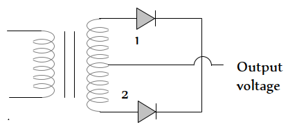
The contribution to output voltage from diode -2 is
- A
$A, C$
- ✓
$B, D$
- C
$B, C$
- D
$A, D$
AnswerCorrect option: B. $B, D$
In the positive half cycle of input ac signal diode $D$ is forward biased and $D$ is reverse biased so in the output voltage signal, $A$ and $C$ are due to $D$. In negative half cycle of lnput $a c$ signal $D$ conducts, hence output signals $B$ and $D$ are due to $D$.
View full question & answer→MCQ 731 Mark
If $n_e$ and $n_h$ are the number of electrons and holes in a semiconductor heavily doped with phosphorus, then
- ✓
$n_e>>n_h$
- B
$n_e\lt n_h$
- C
$n_e \leq n_h$
- D
$n_e=n_h$
AnswerCorrect option: A. $n_e>>n_h$
(a) Phosphorus is a pentavalent impurity so $n>n$.
View full question & answer→MCQ 741 Mark
The majority charge carriers in $P$-type semiconductor are
AnswerIn $P$-type semiconductors, holes are the majority charge carriers
View full question & answer→MCQ 751 Mark
If $N_P$ and $N_e$ be the numbers of holes and conduction electrons in an extrinsic semiconductor, then
AnswerCorrect option: D. $N_{P} ! N_e$ or $N_P \sim N_e$
View full question & answer→MCQ 761 Mark
Resistivity of a semiconductor depends on
- A
- ✓
Atomic nature of semiconductor
- C
- D
Shape and atomic nature of semiconductor
AnswerCorrect option: B. Atomic nature of semiconductor
Resistivity is the intrinsic property, it doesn't depend upon length and shape of the semiconductors.
View full question & answer→MCQ 771 Mark
In a semiconductor, the concentration of electrons is $8 \times 10^{14} / cm ^3$ and that of the holes is $5 \times 10^{12} cm ^3$. The semiconductor is
AnswerCorrect option: B. $N$-type
Since $n>n$; the semiconductor is $N$-type.
View full question & answer→MCQ 781 Mark
Silicon is a semiconductor. If a small amount of $A s$ is added to it, then its electrical conductivity
AnswerImpurity increases the conductivity.
View full question & answer→MCQ 791 Mark
If the forward voltage in a semiconductor diode is doubled, the width of the depletion layer will
MCQ 801 Mark
Wires $P$ and $Q$ have the same resistance at ordinary (room) temperature. When heated, resistance of $P$ increases and that of $Q$ decreases. We conclude that
- A
$P$ and $Q$ are conductors of different materials
- B
$P$ is $N$-type semiconductor and $Q$ is $P$-type semiconductor
- C
$P$ is semiconductor and $Q$ is conductor
- ✓
$P$ is conductor and $Q$ is semiconductor
AnswerCorrect option: D. $P$ is conductor and $Q$ is semiconductor
Conductor has positive temperature coefficient of resistance but semiconductor has negative temperature coefficient of resistance.
View full question & answer→MCQ 811 Mark
The impurity atoms which are mixed with pure silicon to make a $P$ type semiconductor are those of
View full question & answer→MCQ 821 Mark
The forbidden energy band gap in conductors, semiconductors and insulators are $E G_1, E G_2$ and $E G_3$ respectively. The relation among them is
- A
(a) $E G_1=E G_2=E G_3$
- ✓
(b) $E G_1
- C
(c) $E G_1>E G_2>E G_3$
- D
(d) $E G_1E G_3$
AnswerCorrect option: B. (b) $E G_1
(b) In insulators, the forbidden energy gap is very large, in case of semiconductor it is moderate and in conductors the energy gap is zero.
View full question & answer→MCQ 831 Mark
On increasing the reverse bias to a large value in a $P N$-junction diode, current
AnswerAfter a large reverse voltage is $P N$-junction diode, a huge current flows in the reverse direction suddenly. This is called Breakdown of $P N$-junction diode.
View full question & answer→MCQ 841 Mark
In the forward bias arrangement of a $P N$-junction diode
- A
The $N$ end is connected to the positive terminal of the battery
- ✓
The $P$ end is connected to the positive terminal of the battery
- C
The direction of current is from $N$-end to $P$-end in the diode
- D
The $P$ end is connected to the negative terminal of battery
AnswerCorrect option: B. The $P$ end is connected to the positive terminal of the battery
View full question & answer→MCQ 851 Mark
Which statement is correct
- A
N-type germanium is negatively charged and $P$-type germanium is positively charged
- ✓
Both $N$-type and $P$-type germanium are neutral
- C
N-type germanium is positively charged and $P$-type germanium is negatively charged
- D
Both $N$-type and $P$-type germanium are negatively charged
AnswerCorrect option: B. Both $N$-type and $P$-type germanium are neutral
View full question & answer→MCQ 861 Mark
Electrical conductivity of a semiconductor
- A
Decreases with the rise in its temperature
- ✓
Increases with the rise in its temperature
- C
Does not change with the rise in its temperature
- D
First increases and then decreases with the rise in its temperature
AnswerCorrect option: B. Increases with the rise in its temperature
With temperature rise conductivity of semiconductors increases.
View full question & answer→MCQ 871 Mark
The energy gap of silicon is $1.14\ eV$. The maximum wavelength at which silicon will begin absorbing energy is
- ✓
$10888 \mathring A$
- B
$1088.8 \mathring A$
- C
$108.88 \mathring A$
- D
$10.888 \mathring A$
AnswerCorrect option: A. $10888 \mathring A$
$\lambda_{\max }=\frac{h c}{E}=\frac{6.6 \times 10^{-34} \times 3 \times 10^8}{1.14 \times 1.6 \times 10^{-19}}=10888 \mathring A$
View full question & answer→MCQ 881 Mark
Three semi-conductors are arranged in the increasing order of their energy gap as follows. The correct arrangement is
- ✓
Tellurium, germanium, silicon
- B
Tellurium, silicon, germanium
- C
Silicon, germanium, tellurium
- D
Silicon, tellurium, germanium
AnswerCorrect option: A. Tellurium, germanium, silicon
View full question & answer→MCQ 891 Mark
In a triode amplifier, the value of maximum gain is equal to
- A
Half the amplification factor
- ✓
- C
Twice the amplification factor
- D
AnswerThe maximum voltage gain $(A)_{\sim}=\mu$ (Which is obtained when $R=\infty$ ).
View full question & answer→MCQ 901 Mark
The reverse biasing in a $P N$ junction diode
- A
Decreases the potential barrier
- ✓
Increases the potential barrier
- C
Increases the number of minority charge carriers
- D
Increases the number of majority charge carriers
AnswerCorrect option: B. Increases the potential barrier
In reverse biasing, width of depletion layer increases.
View full question & answer→MCQ 911 Mark
The slope of plate characteristic of a vacuum tube diode for certain operating point on the curve is $10^{-3} \frac{ mA }{ V }.$ The plate resistance of the diode and its nature respectively
- A
$100$ kilo-ohms static
- ✓
$1000$ kilo-ohms static
- C
$1000$ kilo-ohms dynamic
- D
$100$ kilo-ohms dynamic
AnswerCorrect option: B. $1000$ kilo-ohms static
$ \text { Plate resistance }=\frac{1}{\text { slope }}=\frac{1}{10^{-3} \times 10^{-3}}=10^6 \Omega$
$ =1000 \mathrm{k} \Omega \text { (static). }$
View full question & answer→MCQ 921 Mark
The valence of an impurity added to germanium crystal in order to convert it into a $P$-type semi conductor is
View full question & answer→MCQ 931 Mark
For a triode, at $V_g=-1$ volt, the following observations were taken $V_p=75 V , I_p=2 mA , V_p=100 V , I_p=4 mA$. The value of plate resistance will be
- A
$25 k \Omega$
- B
$20.8 k \Omega$
- ✓
$12.5 k \Omega$
- D
$100 k \Omega$
AnswerCorrect option: C. $12.5 k \Omega$
$r_p=\frac{V_{p_1}-V_{p_2}}{I_{p_1}-I_{P_2}}=\frac{75-100}{(2-4) \times 10^{-3}}=12.5 \times 10 \Omega=12.5 \mathrm{k} \Omega$.
View full question & answer→MCQ 941 Mark
If the amplification factor of a triode $(\mu)$ is 22 and its plate resistance is $6600 ohm$, then the mutual conductance of this valve is mho is
- ✓
$\frac{1}{300}$
- B
$25 \times 10^{-2}$
- C
$2.5 \times 10^{-2}$
- D
$0.25 \times 10^{-2}$
AnswerCorrect option: A. $\frac{1}{300}$
$\mu=r_p \times g_m \Rightarrow g_m=\frac{\mu}{r_p}=\frac{22}{6600}=\frac{1}{300}$.
View full question & answer→MCQ 951 Mark
In the circuit of a triode valve, there is no change in the plate current, when the plate potential is increased from $200$ volt to $220$ volt and the grid potential is decreased from $-0.5$ volt to $-1.3$ volt. The amplification factor of this valve is
Answer$\mu=\frac{\left(V_{p_1}-V_{p_2}\right.}{\left(V_{G_1}-V_{G_2}\right)}=\frac{(200-220)}{(0.5-1.3)}=25$.
View full question & answer→MCQ 961 Mark
A triode has a mutual conductance of $2 \times 10^{-3} mho$ and an amplification factor of $50.$ The anode is connected through a resistance of $25 \times 10^3$ ohms to a $250$ volts supply. The voltage gain of this amplifier is
Answer$ \text { Using } A_v=\frac{\mu}{1+\frac{r_p}{R_L}} \text { and } \mu=r_p \times g_m$
$\Rightarrow r_p=\frac{\mu}{g_m}=\frac{50}{2 \times 10^{-3}}=25 \times 10^3 \Omega $
$ \therefore A_v=\frac{50}{1+\frac{25 \times 10^3}{25 \times 10^3}}=25 .$
View full question & answer→MCQ 971 Mark
In P-type semiconductor, there is
- A
An excess of one electron
- ✓
- C
- D
AnswerAbsence of one electron, creates the positive charge of magnitude equal to that of electronic charge.
View full question & answer→MCQ 981 Mark
The unit of mutual conductance of a triode valve is
MCQ 991 Mark
AnswerCorrect option: A. Non$-$linear device
Non$-$linear device
View full question & answer→MCQ 1001 Mark
An oscillator is nothing but an amplifier with