MCQ 1011 Mark
The phase difference between input and output voltages of a CE circuit is
MCQ 1021 Mark
At ordinary temperatures, the electrical conductivity of semi conductors in mho/meter is in the range
- A
$10^{-3}$ to $10^{-4}$
- ✓
$10^6$ to $10^9$
- C
$10^{-6}$ to $10^{-10}$
- D
$10^{-10}$ to $10^{-16}$
AnswerCorrect option: B. $10^6$ to $10^9$
View full question & answer→MCQ 1031 Mark
In extrinsic $P$ and $N$-type, semiconductor materials, the ratio of the impurity atoms to the pure semiconductor atoms is about
- A
$1$
- B
$10^1$
- C
$10^4$
- ✓
$10^7$
AnswerCorrect option: D. $10^7$
View full question & answer→MCQ 1041 Mark
When the $P$ end of $P-N$ junction is connected to the negative terminal of the battery and the $N$ end to the positive terminal of the battery, then the $P-N$ junction behaves like
AnswerIn this condition $\mathrm{P}-\mathrm{N}$ junction is reverse biased.
View full question & answer→MCQ 1051 Mark
The approximate ratio of resistances in the forward and reverse bias of the $P N$-junction diode is
- A
$10^2: 1$
- B
$10^{-2}: 1$
- C
$1: 10^{-4}$
- ✓
$1: 10^4$
AnswerCorrect option: D. $1: 10^4$
Resistance in forward biasing $\mathrm{R}_{\mathrm{fr}} \approx 10 \Omega$ and resistance in reverse biasing
$\mathrm{R}_{\mathrm{Rw}} \approx 10^5 \Omega \Rightarrow \frac{\mathrm{R}_{\mathrm{fr}}}{\mathrm{R}_{\mathrm{Rw}}}=\frac{1}{10^4}$
View full question & answer→MCQ 1061 Mark
For germanium crystal, the forbidden energy gap in joules is
- ✓
$1.12 \times 10^{-19}$
- B
$1.76 \times 10^{-19}$
- C
$1.6 \times 10^{-19}$
- D
AnswerCorrect option: A. $1.12 \times 10^{-19}$
For Ge, $E_g=0.7 \mathrm{eV}=0.7 \times 1.6 \times 10^{-19} \mathrm{~J}=1.12 \times 10^{-19} \mathrm{~J}$
View full question & answer→MCQ 1071 Mark
To obtain electrons as majority charge carriers in a semiconductor, the impurity mixed is
MCQ 1081 Mark
A semiconductor is cooled from $T_1 K$ to $T_2 K$. Its resistance
- A
- ✓
- C
Will first decrease and then increase
- D
View full question & answer→MCQ 1091 Mark
Electronic configuration of germanium is $2,8,18$ and $4$ . To make it extrinsic semiconductor small quantity of antimony is added
- A
The material obtained will be $N-$type germanium in which electrons and holes are equal in number
- B
The material obtained will be $P-$type germanium
- ✓
The material obtained will be $N-$type germanium which has more electrons than holes at room temperature
- D
The material obtained will be $N-$type germanium which has less electrons than holes at room temperature
AnswerCorrect option: C. The material obtained will be $N-$type germanium which has more electrons than holes at room temperature
The material obtained will be $N-$type germanium which has more electrons than holes at room temperature
View full question & answer→MCQ 1101 Mark
At zero Kelvin a piece of germanium
AnswerAt zero Kelvin, there is no thermal agitation and therefore no electrons from valence band are able to shift to conduction band.
View full question & answer→MCQ 1111 Mark
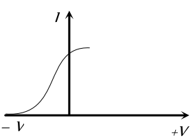
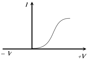
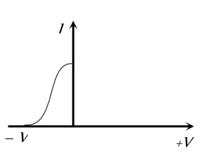
Different voltages are applied across a $P-N$ junction and the currents are measured for each value. Which of the following graphs is obtained between voltage and current
Answer$P N$ junction has low resistance in one direction of potential difference $+V$, so a large current flows (forward biasing). It has a high resistance in the opposite potential difference direction $-V$, so a very small current flows (Reverse biasing).
View full question & answer→MCQ 1121 Mark
A hole in a $P$-type semiconductor is
View full question & answer→MCQ 1131 Mark
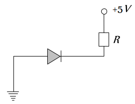
A semiconductor device is connected in a series circuit with a battery and a resistance. A current is found to pass through the circuit. If the polarity of the battery is reversed, the current drops almost to zero. The device may be
- A
A $P$-type semiconductor
- B
- ✓
A $P N$-junction
- D
An intrinsic semiconductor
AnswerCorrect option: C. A $P N$-junction
When polarity of the battery is reversed, the $P-N$ junction becomes reverse biased so no current flows.
View full question & answer→MCQ 1141 Mark
Let $n_P$ and $n_e$ be the number of holes and conduction electrons respectively in a semiconductor. Then
- A
(a) $n_{P} ! n_e$ in an intrinsic semiconductor
- B
(b) $n_P \quad n_e$ in an extrinsic semiconductor
- ✓
(c) $n_P \quad n_e$ in an intrinsic semiconductor
- D
(d) $n_{e} ! n_P$ in an intrinsic semiconductor
AnswerCorrect option: C. (c) $n_P \quad n_e$ in an intrinsic semiconductor
(c) In intrinsic semiconductors, the creation or liberation of one free electron by the thermal energy has created one hole. Thus in intrinsic semiconductors $n=n$.
View full question & answer→MCQ 1151 Mark
The energy band gap of $S i$ is
AnswerCorrect option: B. $1.1\ eV$
View full question & answer→MCQ 1161 Mark
In a $P N$-junction diode
- ✓
The current in the reverse biased condition is generally very small
- B
The current in the reverse biased condition is small but the forward biased current is independent of the bias voltage
- C
The reverse biased current is strongly dependent on the applied bias voltage
- D
The forward biased current is very small in comparison to reverse biased current
AnswerCorrect option: A. The current in the reverse biased condition is generally very small
In forward biased $P N$-junction, external voltage decreases the potential barrier, so current is maximum. While in reversed biased $P N$-junction, external voltage increases the potential barrier, so the current is very small.
View full question & answer→MCQ 1171 Mark
- A
If the grid voltage is zero then plate current will be zero
- B
If the temperature of filament is doubled, then the thermionic current will also be doubled
- ✓
If the temperature of filament is doubled, then the thermionic current will nearly be four times
- D
At a definite grid voltage the plate current varies with plate voltage according to Ohm's law
AnswerCorrect option: C. If the temperature of filament is doubled, then the thermionic current will nearly be four times
View full question & answer→MCQ 1181 Mark
Which is the wrong statement in following sentences? A device in which $P$ and $N$-type semiconductors are used is more useful then a vacuum type because
- A
Power is not necessary to heat the filament
- B
- C
Very less heat is produced in it
- ✓
Its efficiency is high due to a high voltage across the junction
AnswerCorrect option: D. Its efficiency is high due to a high voltage across the junction
View full question & answer→MCQ 1191 Mark
With a change of load resistance of a triode, used as an amplifier, from $50$ kilo ohms to $100$ kilo ohms, its voltage amplification changes from $25$ to $30.$ Plate resistance of the triode is
- ✓
$25 k \Omega$
- B
$75 k \Omega$
- C
$7.5 k \Omega$
- D
$2.5 k \Omega$
AnswerCorrect option: A. $25 k \Omega$
$ \text { Voltage amplification } A_v=\frac{\mu}{1+\frac{r_p}{R_L}}$
$ \Rightarrow 25=\frac{\mu}{1+\frac{r_p}{50 \times 10^3}}$
and $30=\frac{\mu}{1+\frac{r_p}{100 \times 10^3}}$an solving equation (i) and (ii), $r_p=25 \mathrm{k} \Omega$.
View full question & answer→MCQ 1201 Mark
In a triode, $g_m=2 \times 10^{-3} ohm ^{-1} ; \mu=42$, resistance load, $R=50$ kilo ohm. The voltage amplification obtained from this triode will be
- A
$30.42$
- ✓
$29.57$
- C
$28.18$
- D
$ 27.15$
AnswerCorrect option: B. $29.57$
$ \text { Voltage gain } A_v=\frac{\mu}{1+\frac{r_p}{R_L}} \text { and } \mu=r_p \times g_m$
$ \Rightarrow r_p=\frac{42}{2 \times 10^{-3}}=21000 \Omega$
$ \Rightarrow A_v=\frac{42}{1+\frac{21000}{50 \times 10^3}}=29.57$
View full question & answer→MCQ 1211 Mark
The grid voltage of any triode valve is changed from $-1$ volt to $-3$ volt and the mutual conductance is $3 \times 10^{-4} mho$. The change in plate circuit current will be
- A
$0.8 mA$
- ✓
$0.6 mA$
- C
$0.4 mA$
- D
$1 mA$
AnswerCorrect option: B. $0.6 mA$
$ \text { By using } g_m=\frac{\Delta i_p}{\Delta v_g} \Rightarrow 3 \times 10^{-4}=\frac{\Delta i_p}{-1-(-3)} $
$ \Rightarrow \Delta i_p=6 \times 10^{-4} \mathrm{~A}=0.6 \mathrm{~mA}$
View full question & answer→MCQ 1221 Mark
The most commonly used material for making transistor is
MCQ 1231 Mark
In an experiment, the saturation in the plate current in a diode is observed at $240 V$. But a student still wants to increase the plate current. It can be done, if
- A
The plate voltage is increased further
- B
The plate voltage is decreased
- C
The filament current is decreased
- ✓
The filament current is increased
AnswerCorrect option: D. The filament current is increased
After saturation plate current can be increased by increasing the temperature of filament. It can be done by increasing the filament current.
View full question & answer→MCQ 1241 Mark
The valence of the impurity atom that is to be added to germanium crystal so as to make it a $N$-type semiconductor, is
View full question & answer→MCQ 1251 Mark
The amplification factor of a triode is $20.$ Its plate resistance is $10$ kilo ohms. Mutual conductance is
- A
$2 \times 10^5 mho$
- B
$2 \times 10^4 mho$
- C
$500\ mho$
- ✓
$2 \times 10^{-3} mho$
AnswerCorrect option: D. $2 \times 10^{-3} mho$
Using $\mu=r_p \times g_m \Rightarrow g_m=\frac{20}{10 \times 10^3}=2 \times 10^{-3}$.
View full question & answer→MCQ 1261 Mark
In a $P$-type semi-conductor, germanium is dopped with
AnswerGallium, boron and aluminum are trivalent.
View full question & answer→MCQ 1271 Mark
The process of adding impurities to the pure semiconductor is called
MCQ 1281 Mark
Semiconductor is damaged by the strong current due to
AnswerWhen a strong current passes through the semiconductor it heats up the crystal and covalent bond are broken. Hence because of excess number of free electrons it behaves like a conductor.
View full question & answer→MCQ 1291 Mark
In NPN transistor the collector current is $10\ mA$. If $90 \%$ of electrons emitted reach the collector, then
- A
Emitter current will be $9 mA$
- ✓
Emitter current will be $11.1 mA$
- C
Base current will be $0.1 mA$
- D
Base current will be $0.01 mA$
AnswerCorrect option: B. Emitter current will be $11.1 mA$
View full question & answer→MCQ 1301 Mark
In an $N P N$ transistor the collector current is $24 mA$. If $80 \%$ of electrons reach collector its base current in $m A$ is
AnswerGiven $i_c=\frac{80}{100} \times i_e \Rightarrow 24=\frac{80}{100} \times i_e \Rightarrow i_e=30 \mathrm{~mA}$
By using $i_e=i_b+i_c \Rightarrow i=30-24=6 \mathrm{~mA}$.
View full question & answer→MCQ 1311 Mark
At room temperature, a $P$-type semiconductor has
- ✓
Large number of holes and few electrons
- B
Large number of free electrons and few holes
- C
Equal number of free electrons and holes
- D
AnswerCorrect option: A. Large number of holes and few electrons
In $P$-type semi conductor, holes are majority charge carriers.
View full question & answer→MCQ 1321 Mark
In the given figure, which of the diodes are forward biased ?
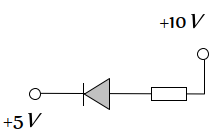
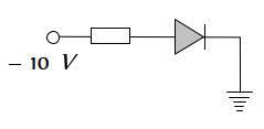
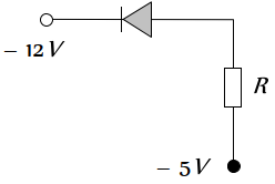
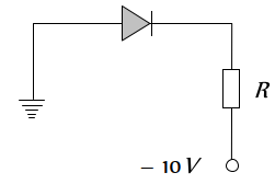
- A
- ✓
- C
(c) $1,3,4$
- D
(d) $2,3,4$
Answer(b) In figure 2,4 and 5. P-crystals are more positive as compared to $N$-crystals.
View full question & answer→MCQ 1331 Mark
The emitter-base junction of a transistor is biased while the collector-base junction is biased
AnswerThe emitter base junction is forward biased while collector base junction is reversed biased.
View full question & answer→MCQ 1341 Mark
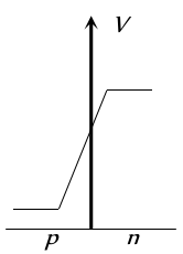
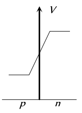
In a forward biased $P N$-ju nction diode, the potential barrier in the depletion region is of the form ...
AnswerPotential across the $P N$ junction varies symmetrically linear, having $P$ side negative and $N$ side positive.
View full question & answer→MCQ 1351 Mark
The electrical circuit used to get smooth $d c$ output from a rectifier circuit is called
AnswerFilter circuits are used to get smooth $d c \pi$-filter is the best filter.
View full question & answer→MCQ 1361 Mark
If $l_1, l_2, l_3$ are the lengths of the emitter, base and collector of a transistor then
- A
(a) $l_1=l_2=l_3$
- B
(b) $l_3l_1$
- C
(c) $l_3
- ✓
(d) $l_3>l_1>l_2$
AnswerCorrect option: D. (d) $l_3>l_1>l_2$
View full question & answer→MCQ 1371 Mark
In an NPN transistor circuit, the collector current is $10 mA$. If $90 \%$ of the electrons emitted reach the collector, the emitter current ( $i$ ) and base current $(i)$ are given by
- A
$i=-1 mA , i=9 mA$
- B
$i=9 m A, i=-1 m A$
- C
$i=1 mA , i=11 mA$
- ✓
$i=11 mA , i=1 mA$
AnswerCorrect option: D. $i=11 mA , i=1 mA$
$i_C=\frac{90}{100} \times i_E \Rightarrow 10=0.9 \times i_c=11 \mathrm{~mA}$
Also $i_E=i_B+i_C \Rightarrow i_B=11-10=1 \mathrm{~mA}$.
View full question & answer→MCQ 1381 Mark
The electrical circuits used to get smooth d.c. output from a rectifier circuit is called
MCQ 1391 Mark
Least doped region in a transistor
- A
Either emitter or collector
- ✓
- C
- D
AnswerIn transistor, base is least doped.
View full question & answer→MCQ 1401 Mark
In the depletion region of an unbiased $P-N$ junction diode there are
View full question & answer→MCQ 1411 Mark
The impurity atom added to germanium to make it $N$-type semiconductor is
AnswerFor $N$-type semiconductor, the impurity should be pentavalent.
View full question & answer→MCQ 1421 Mark
In a good conductor the energy gap between the conduction band and the valence band is
AnswerThe conduction and valence bands in the conductors merge into each other.
View full question & answer→MCQ 1431 Mark
When a semiconductor is heated, its resistance
MCQ 1441 Mark
In a transistor in $CE$ configuration, the ratio of power gain to voltage gain is
- A
$\alpha$
- B
$\beta / \alpha$
- C
$\beta \alpha$
- ✓
$\beta$
AnswerCorrect option: D. $\beta$
For CE configuration voltage gain $=\beta \times R_L / R_i$
Power gain $=\beta^2 \times R_L / R_i $
$\Rightarrow \frac{\text { Power gain }}{\text { Voltage gain }}=\beta$
View full question & answer→MCQ 1451 Mark
$N P N$ transistor are preferred to $P N P$ transistor because they have
- A
- B
- C
Capability of handing large power
- ✓
Electrons having high mobility than holes
AnswerCorrect option: D. Electrons having high mobility than holes
View full question & answer→MCQ 1461 Mark
The maximum efficiency of full wave rectifier is
- A
$100 \%$
- B
$25.20 \%$
- C
$40.2 \%$
- ✓
$81.2 \%$
AnswerCorrect option: D. $81.2 \%$
$\text { For full wave rectifier } \eta=\frac{81.2}{1+\frac{r_f}{R_L}} $
$ \Rightarrow n_{\max }=81.2 \% \quad(r \ll R)$
View full question & answer→MCQ 1471 Mark
In intrinsic semiconductor at room temperature, number of electrons and holes are
AnswerIn intrinsic semiconductors, at room temperature $n=n$.
View full question & answer→MCQ 1481 Mark
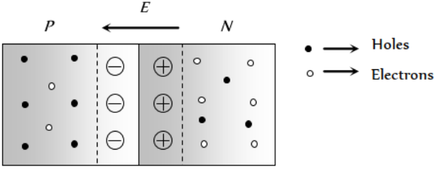
In a $P N$-junction diode not connected to any circuit
- A
The potential is the same everywhere
- B
The $P$-type is a higher potential than the $N$-type side
- ✓
There is an electric field at the junction directed from the $N$ type side to the $P$-type side
- D
There is an electric field at the junction directed from the $P$ type side to the $N$-type side
AnswerCorrect option: C. There is an electric field at the junction directed from the $N$ type side to the $P$-type side
At junction a potential barrier/depletion layer is formed, with $N$-side at higher potential and $P$-side at lower potential.
Therefore there is an electric field at the junction directed from the $N$-side to $P$-side
View full question & answer→MCQ 1491 Mark
Which of the following statements is not true
- A
The resistance of intrinsic semiconductors decrease with increase of temperature
- B
Doping pure $S i$ with trivalent impurities give $P$-type semiconductors
- ✓
The majority carriers in $N$-type semiconductors are holes
- D
A $P N$-junction can act as a semiconductor diode
AnswerCorrect option: C. The majority carriers in $N$-type semiconductors are holes
In $N$-type semiconductor majority charge carriers are electrons.
View full question & answer→MCQ 1501 Mark
The dominant mechanisms for motion of charge carriers in forward and reverse biased silicon $P-N$ junctions are
- A
Drift in forward bias, diffusion in reverse bias
- ✓
Diffusion in forward bias, drift in reverse bias
- C
Diffusion in both forward and reverse bias
- D
Drift in both forward and reverse bias
AnswerCorrect option: B. Diffusion in forward bias, drift in reverse bias
In forward biasing the diffusion current increases and drift current remains constant so not current is due to the diffusion.In reverse biasing diffusion becomes more difficult so net current (very small) is due to the drift.
View full question & answer→