MCQ 11 Mark
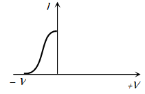
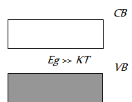
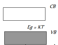
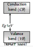
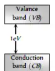
Assertion : A P-N photodiode is made from a semiconductor for which $E_g=2.8 \mathrm{~eV}$. This photo diode will not detect the wavelength of 6000 nm.
Reason : A PN photodiode detect wavelength l if $\frac{h c}{\lambda}>E_e$.
- ✓
If both assertion and reason are true and the reason is the correct explanation of the assertion.
- B
If both assertion and reason are true but reason is not the correct explanation of the assertion.
- C
If assertion is true but reason is false.
- D
If the assertion and reason both are false.
AnswerCorrect option: A. If both assertion and reason are true and the reason is the correct explanation of the assertion.
(a) If both assertion and reason are true and the reason is the correct explanation of the assertion.
View full question & answer→MCQ 21 Mark
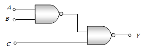
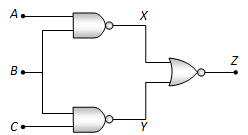
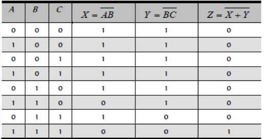
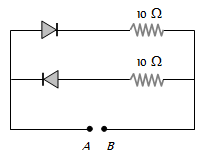
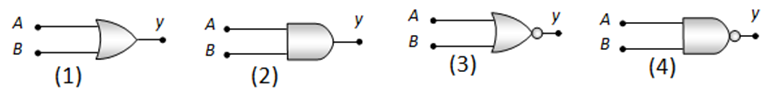
Assertion : De-morgan's theorem $\overline{A+B}=\bar{A} \cdot \bar{B}$ may be explained by the following circuit
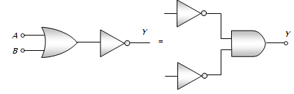
Reason : In the following circuit, for output inputs ABC are 101
- A
If both assertion and reason are true and the reason is the correct explanation of the assertion.
- B
If both assertion and reason are true but reason is not the correct explanation of the assertion.
- ✓
If assertion is true but reason is false.
- D
If the assertion and reason both are false.
AnswerCorrect option: C. If assertion is true but reason is false.
If assertion is true but reason is false.
View full question & answer→MCQ 31 Mark
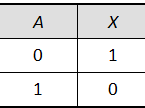
Assertion $: 29$ is the equivalent decimal number of binary number $11101.$
Reason $:(11101)_2=\left(1 \times 2^4+1 \times 2^3+1 \times 2^2+0 \times 2^1+1 \times 2^0\right)_{10}=(16+8+4+0+1)_{10}=(29)_{10}$
- ✓
If both assertion and reason are true and the reason is the correct explanation of the assertion.
- B
If both assertion and reason are true but reason is not the correct explanation of the assertion.
- C
If assertion is true but reason is false.
- D
If the assertion and reason both are false.
AnswerCorrect option: A. If both assertion and reason are true and the reason is the correct explanation of the assertion.
If both assertion and reason are true and the reason is the correct explanation of the assertion.
View full question & answer→MCQ 41 Mark
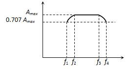
The frequency response curve of RC coupled amplifier is shown in figure. The band width of the amplifier will be
- A
$f_3-f_2$
- ✓
$f_4-f_1$
- C
$\frac{f_4-f_2}{2}$
- D
$f_3-f_1$
AnswerCorrect option: B. $f_4-f_1$
(b) $f_4-f_1$
View full question & answer→MCQ 51 Mark
Assertion : NOT gate is also called inverter circuit.
Reason : NOT gate inverts the input order.
- ✓
If both assertion and reason are true and the reason is the correct explanation of the assertion.
- B
If both assertion and reason are true but reason is not the correct explanation of the assertion.
- C
If assertion is true but reason is false.
- D
If the assertion and reason both are false.
AnswerCorrect option: A. If both assertion and reason are true and the reason is the correct explanation of the assertion.
If both assertion and reason are true and the reason is the correct explanation of the assertion.
View full question & answer→MCQ 61 Mark
Assertion : Zener diode works on a principle of breakdown voltage.
Reason : Current increases suddenly after breakdown voltage.
- ✓
If both assertion and reason are true and the reason is the correct explanation of the assertion.
- B
If both assertion and reason are true but reason is not the correct explanation of the assertion.
- C
If assertion is true but reason is false.
- D
If the assertion and reason both are false.
AnswerCorrect option: A. If both assertion and reason are true and the reason is the correct explanation of the assertion.
If both assertion and reason are true and the reason is the correct explanation of the assertion.
View full question & answer→MCQ 71 Mark
Assertion : V-i characteristic of P-N junction diode is same as that of any other conductor.
Reason : P-N junction diode behave as conductor at room temperature.
- A
If both assertion and reason are true and the reason is the correct explanation of the assertion.
- B
If both assertion and reason are true but reason is not the correct explanation of the assertion.
- C
If assertion is true but reason is false.
- ✓
If the assertion and reason both are false.
AnswerCorrect option: D. If the assertion and reason both are false.
If the assertion and reason both are false.
View full question & answer→MCQ 81 Mark
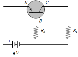
Assertion : Base in a transistor is made very thin as compared to collector and emitter regions.
Reason : Due to thin base power gain and voltage gain is obtained by a transistor.
- ✓
If both assertion and reason are true and the reason is the correct explanation of the assertion.
- B
If both assertion and reason are true but reason is not the correct explanation of the assertion.
- C
If assertion is true but reason is false.
- D
If the assertion and reason both are false.
AnswerCorrect option: A. If both assertion and reason are true and the reason is the correct explanation of the assertion.
If both assertion and reason are true and the reason is the correct explanation of the assertion.
View full question & answer→MCQ 91 Mark
Assertion : At 0 K Germanium is a superconductor.
Reason : At 0 K Germanium offers zero resistance.
- A
If both assertion and reason are true and the reason is the correct explanation of the assertion.
- B
If both assertion and reason are true but reason is not the correct explanation of the assertion.
- C
If assertion is true but reason is false.
- ✓
If the assertion and reason both are false.
AnswerCorrect option: D. If the assertion and reason both are false.
If the assertion and reason both are false.
View full question & answer→MCQ 101 Mark
Assertion : NAND or NOR gates are called digital building blocks.
Reason : The repeated use of NAND (or NOR) gates can produce all the basic or complicated gates.
- ✓
If both assertion and reason are true and the reason is the correct explanation of the assertion.
- B
If both assertion and reason are true but reason is not the correct explanation of the assertion.
- C
If assertion is true but reason is false.
- D
If the assertion and reason both are false.
AnswerCorrect option: A. If both assertion and reason are true and the reason is the correct explanation of the assertion.
If both assertion and reason are true and the reason is the correct explanation of the assertion.
View full question & answer→MCQ 111 Mark
Assertion : A transistor is a voltage-operating device.
Reason : Base current is greater than the collector current.
- A
If both assertion and reason are true and the reason is the correct explanation of the assertion.
- B
If both assertion and reason are true but reason is not the correct explanation of the assertion.
- C
If assertion is true but reason is false.
- ✓
If the assertion and reason both are false.
AnswerCorrect option: D. If the assertion and reason both are false.
If the assertion and reason both are false.
View full question & answer→MCQ 121 Mark
Assertion : In transistor common emitter mode as an amplifier is preferred over common base mode.
Reason : In common emitter mode the input signal is connected in series with the voltage applied to the base emitter function.
- A
If both assertion and reason are true and the reason is the correct explanation of the assertion.
- ✓
If both assertion and reason are true but reason is not the correct explanation of the assertion.
- C
If assertion is true but reason is false.
- D
If the assertion and reason both are false.
AnswerCorrect option: B. If both assertion and reason are true but reason is not the correct explanation of the assertion.
If both assertion and reason are true but reason is not the correct explanation of the assertion.
View full question & answer→MCQ 131 Mark
Assertion : Two P-N junction diodes placed back to back, will work as a NPN transistor.
Reason : The P-region of two PN junction diodes back to back will form the base of NPN transistor.
- A
If both assertion and reason are true and the reason is the correct explanation of the assertion.
- B
If both assertion and reason are true but reason is not the correct explanation of the assertion.
- C
If assertion is true but reason is false.
- ✓
If the assertion and reason both are false.
AnswerCorrect option: D. If the assertion and reason both are false.
If the assertion and reason both are false.
View full question & answer→MCQ 141 Mark
Assertion : Semiconductors do not Obey's Ohm's law.
Reason : Current is determined by the rate of flow of charge carriers.
- A
If both assertion and reason are true and the reason is the correct explanation of the assertion.
- B
If both assertion and reason are true but reason is not the correct explanation of the assertion.
- C
If assertion is true but reason is false.
- ✓
If assertion is false but reason is true.
AnswerCorrect option: D. If assertion is false but reason is true.
If assertion is false but reason is true.
View full question & answer→MCQ 151 Mark
Assertion : We can measure the potential barrier of a PN junction by putting a sensitive voltmeter across its terminals.
Reason : The current through the PN junction is not same in forward and reversed bias.
- A
If both assertion and reason are true and the reason is the correct explanation of the assertion.
- B
If both assertion and reason are true but reason is not the correct explanation of the assertion.
- C
If assertion is true but reason is false.
- ✓
If assertion is false but reason is true.
AnswerCorrect option: D. If assertion is false but reason is true.
If assertion is false but reason is true.
View full question & answer→MCQ 161 Mark
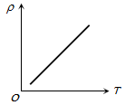
Assertion : Silicon is preferred over germanium for making semiconductor devices.
Reason : The energy gap for germanium is more than the energy gap of silicon.
- A
If both assertion and reason are true and the reason is the correct explanation of the assertion.
- B
If both assertion and reason are true but reason is not the correct explanation of the assertion.
- ✓
If assertion is true but reason is false.
- D
If the assertion and reason both are false.
AnswerCorrect option: C. If assertion is true but reason is false.
If assertion is true but reason is false.
View full question & answer→MCQ 171 Mark
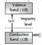
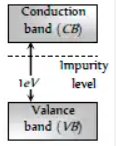
Assertion : An N-type semiconductor has a large number of electrons but still it is electrically neutral.
Reason : An N-type semiconductor is obtained by doping an intrinsic semiconductor with a pentavalent impurity.
- A
If both assertion and reason are true and the reason is the correct explanation of the assertion.
- ✓
If both assertion and reason are true but reason is not the correct explanation of the assertion.
- C
If assertion is true but reason is false.
- D
If the assertion and reason both are false.
AnswerCorrect option: B. If both assertion and reason are true but reason is not the correct explanation of the assertion.
If both assertion and reason are true but reason is not the correct explanation of the assertion.
View full question & answer→MCQ 181 Mark
Assertion : Electron has higher mobility than hole in a semiconductor.
Reason : Mass of electron is less than the mass of hole.
- ✓
If both assertion and reason are true and the reason is the correct explanation of the assertion.
- B
If both assertion and reason are true but reason is not the correct explanation of the assertion.
- C
If assertion is true but reason is false.
- D
If the assertion and reason both are false.
AnswerCorrect option: A. If both assertion and reason are true and the reason is the correct explanation of the assertion.
If both assertion and reason are true and the reason is the correct explanation of the assertion.
View full question & answer→MCQ 191 Mark
Assertion : The temperature coefficient of resistance is positive for metals and negative for P-type semiconductor.
Reason : The effective charge carriers in metals are negatively charged whereas in P-type semiconductor they are positively charged.
- A
If both assertion and reason are true and the reason is the correct explanation of the assertion.
- ✓
If both assertion and reason are true but reason is not the correct explanation of the assertion.
- C
If assertion is true but reason is false.
- D
If the assertion and reason both are false.
AnswerCorrect option: B. If both assertion and reason are true but reason is not the correct explanation of the assertion.
If both assertion and reason are true but reason is not the correct explanation of the assertion.
View full question & answer→MCQ 201 Mark
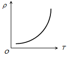
Assertion : If the temperature of a semiconductor is increased then it's resistance decreases.
Reason : The energy gap between conduction band and valence band is very small
- ✓
If both assertion and reason are true and the reason is the correct explanation of the assertion
- B
If both assertion and reason are true but reason is not the correct explanation of the assertion.
- C
If assertion is true but reason is false
- D
If the assertion and reason both are false.
AnswerCorrect option: A. If both assertion and reason are true and the reason is the correct explanation of the assertion
If both assertion and reason are true and the reason is the correct explanation of the assertion.
View full question & answer→MCQ 211 Mark
Assertion : The resistivity of a semiconductor increases with temperature.
Reason : The atoms of a semiconductor vibrate with larger amplitude at higher temperature there by increasing it's resistivity.
- A
If both assertion and reason are true and the reason is the correct explanation of the assertion.
- ✓
If both assertion and reason are true but reason is not the correct explanation of the assertion.
- C
If assertion is true but reason is false.
- D
If the assertion and reason both are false.
AnswerCorrect option: B. If both assertion and reason are true but reason is not the correct explanation of the assertion.
If the assertion and reason both are false.
View full question & answer→MCQ 221 Mark
Assertion : A transistor amplifier in common emitter configuration has a low input impedence.
Reason : The base to emitter region is forward biased.
- ✓
If both assertion and reason are true and the reason is the correct explanation of the assertion.
- B
If both assertion and reason are true but reason is not the correct explanation of the assertion.
- C
If assertion is true but reason is false
- D
If the assertion and reason both are false.
AnswerCorrect option: A. If both assertion and reason are true and the reason is the correct explanation of the assertion.
If both assertion and reason are true and the reason is the correct explanation of the assertion.
View full question & answer→MCQ 231 Mark
Assertion : In a common emitter transistor amplifier the input current is much less than the output current.
Reason : The common emitter transistor amplifier has very high input impedance.
- A
If both assertion and reason are true and the reason is the correct explanation of the assertion.
- B
If both assertion and reason are true but reason is not the correct explanation of the assertion.
- ✓
If assertion is true but reason is false.
- D
If the assertion and reason both are false.
AnswerCorrect option: C. If assertion is true but reason is false.
(c) If assertion is true but reason is false.
View full question & answer→MCQ 241 Mark
Assertion : The number of electrons in a P-type silicon semiconductor is less than the number of electrons in a pure silicon semiconductor at room temperature.
Reason : It is due to law of mass action.
- ✓
If both assertion and reason are true and the reason is the correct explanation of the assertion.
- B
If both assertion and reason are true but reason is not the correct explanation of the assertion.
- C
If assertion is true but reason is false.
- D
If the assertion and reason both are false.
AnswerCorrect option: A. If both assertion and reason are true and the reason is the correct explanation of the assertion.
(a) If both assertion and reason are true and the reason is the correct explanation of the assertion.
View full question & answer→MCQ 251 Mark
The output current versus time curve of a rectifier is shown in the figure. The average value of the output current in this case is
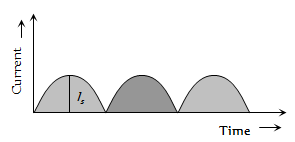
AnswerCorrect option: C. $2 \mathrm{i}_0 / \mathrm{p}$
(c) $2 \mathrm{i}_0 / \mathrm{p}$
View full question & answer→MCQ 261 Mark
Assertion : When PN-junction is forward biased then motion of charge carriers at junction is due to diffusion. In reverse biasing. The cause of motion of charge is drifting.
Reason : In the following circuit emitter is reverse biased and collector is forward biased.
- A
If both assertion and reason are true and the reason is the correct explanation of the assertion.
- ✓
If both assertion and reason are true but reason is not the correct explanation of the assertion.
- C
If assertion is true but reason is false.
- D
If the assertion and reason both are false.
AnswerCorrect option: B. If both assertion and reason are true but reason is not the correct explanation of the assertion.
(b) If both assertion and reason are true but reason is not the correct explanation of the assertion.
View full question & answer→MCQ 271 Mark
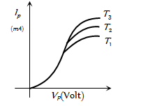
For the diode, the characteristic curves are given at different temperature. The relation between the temperatures is
- A
$\mathrm{T}_1=\mathrm{T}_2=\mathrm{T}_3$
- ✓
$\mathrm{T}_1<\mathrm{T}_2<\mathrm{T}_3$
- C
$\mathrm{T}_1>\mathrm{T}_2>\mathrm{T}_3$
- D
AnswerCorrect option: B. $\mathrm{T}_1<\mathrm{T}_2<\mathrm{T}_3$
(b) $\mathrm{T}_1<\mathrm{T}_2<\mathrm{T}_3$
View full question & answer→MCQ 281 Mark
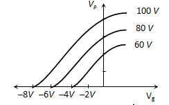
The mutual characteristic curves of a triode are as shown in figure. The cut off voltage for the triode is
MCQ 291 Mark
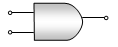
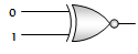
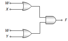
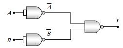
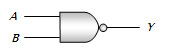
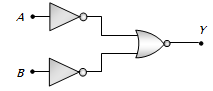
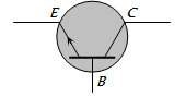
Assertion : The following circuit represents 'OR' gate
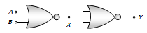
Reason : For the above circuit $Y=\bar{X}=\overline{\overline{A+B}}=A+B$ - ✓
If both assertion and reason are true and the reason is the correct explanation of the assertion.
- B
If both assertion and reason are true but reason is not the correct explanation of the assertion.
- C
If assertion is true but reason is false.
- D
If the assertion and reason both are false.
AnswerCorrect option: A. If both assertion and reason are true and the reason is the correct explanation of the assertion.
(a) If both assertion and reason are true and the reason is the correct explanation of the assertion.
View full question & answer→MCQ 301 Mark
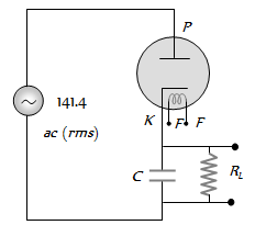
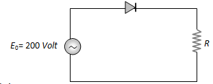
An alternating voltage of 141.4V (rms) is applied to a vacuum diode as shown in the figure. The maximum potential difference across the condenser will be.
- A
- ✓
- C
100$\sqrt {2}V$
- D
200$\sqrt {2}V$
View full question & answer→MCQ 311 Mark
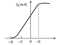
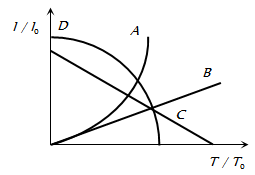
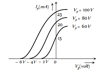
The ratio of thermionic currents ($l / l_0$) for a metal when the temperature is slowly increased $T_0$ to T as shown in figure. (l and $\mathrm{l}_0$ are currents at T and respectively). Then which one is correct?
View full question & answer→MCQ 321 Mark
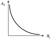
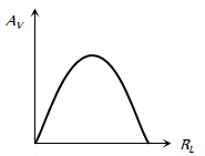
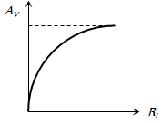
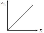
The correct curve between voltage gain $(A_L)$and load resistance $(R_L) $ is
Answer(c)

View full question & answer→MCQ 331 Mark
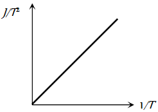
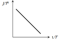
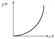
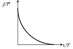
If the thermionic current density is J and emitter temperature is T then the curve between $\frac{J}{T_2}$ and $\frac{1}{T}$ will be
Answer(c)
View full question & answer→MCQ 341 Mark
The point representing the cut off grid voltage on the mutual characteristic of triode is
MCQ 351 Mark
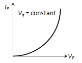
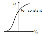
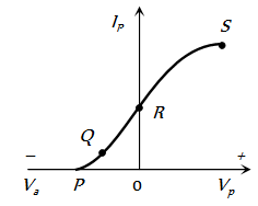
The relation between $I_p$ and $V_p$ for a triode is $\mathrm{I}_{\mathrm{p}}=\left(0.125 \mathrm{V}_{\mathrm{p}}-7.5\right) \mathrm{mA}$ , Keeping the grid potential constant at 1V, the value of $r_p$ will be
- A
$8 \mathrm{k} \Omega$
- B
$4 \mathrm{k} \Omega$
- C
$2 \mathrm{k} \Omega$
- ✓
$8 \mathrm{k} \Omega$
AnswerCorrect option: D. $8 \mathrm{k} \Omega$
(d) $8 \mathrm{k} \Omega$
View full question & answer→MCQ 361 Mark
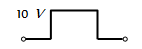
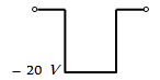
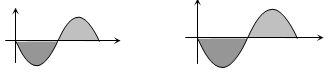
The given figure shows the wave forms for two inputs A and B and that for the output Y of a logic circuit. The logic circuit is
MCQ 371 Mark
The output in the circuit of figure is taken across a capacitor. It is as shown in figure
Answer(c)

View full question & answer→MCQ 381 Mark
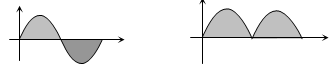
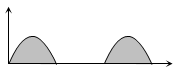
In the half-wave rectifier circuit shown. Which one of the following wave forms is true for $\mathrm{V}_\mathrm{CD}$, the output across C and D ?
Answer(b)
View full question & answer→MCQ 391 Mark
The resistance of a germanium junction diode whose $V - I$ is shown in figure is $\left( v _{ k }=0.3 v \right)$
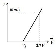
AnswerCorrect option: B. $0.2 \ kW$
(b) $0.2 \ kW$
View full question & answer→MCQ 401 Mark
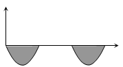
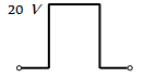
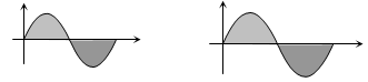
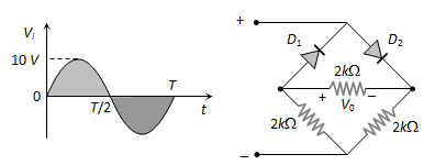
If the following input signal is sent through a PN-junction diode, then the output signal across $R_L$ will be
Answer(c)

View full question & answer→MCQ 411 Mark
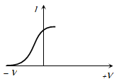
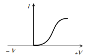
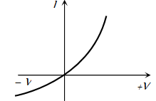
Different voltages are applied across a P-N junction and the currents are measured for each value. Which of the following graphs is obtained between voltage and current
Answer(c)
View full question & answer→MCQ 421 Mark
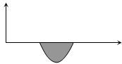
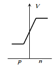
In a forward biased PN-junction diode, the potential barrier in the depletion region is of the form …
Answer(b)
View full question & answer→MCQ 431 Mark
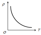
The temperature (T) dependence of resistivity (r) of a semiconductor is represented by
Answer(c)
View full question & answer→MCQ 441 Mark
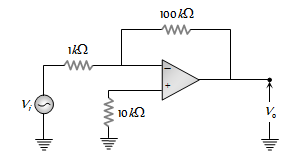
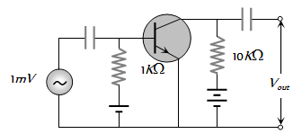
The voltage gain of the following amplifier is
MCQ 451 Mark
The slopes of anode and mutual characteristics of a triode are $0.02 \ mA\ V^{-1}$ and 1 mA $V^{-1}$ respectively. What is the amplification factor of the valve
View full question & answer→MCQ 461 Mark
Amplification factor of a triode is 10. When the plate potential is 200 volt and grid potential is – 4 volt, then the plate current of 4mA is observed. If plate potential is changed to 160 volt and grid potential is kept at – 7 volt, then the plate current will be
MCQ 471 Mark
For a triode $m = 64$ and $g_m=1600$ m mho. It is used as an amplifier and an input signal of $1V ($rms$)$ is applied. The signal power in the load of $40 kW$ will be
- A
$23.5 \ mW$
- B
$48.7 \ mW$
- ✓
$25.6 \ mW$
- D
AnswerCorrect option: C. $25.6 \ mW$
$25.6 \ mW$
View full question & answer→MCQ 481 Mark
In the grid circuit of a triode a signal $E=2 \sqrt{2} \cos \omega t$ is applied. If $m=14$ and $r_p=10 kW$ then root mean square current flowing through $R _{ L }=12 k \Omega$ will be
- ✓
$1.27 \ mA$
- B
$10 \ mA$
- C
$1.5 \ mA$
- D
$12.4 \ mA$
AnswerCorrect option: A. $1.27 \ mA$
(a) $1.27 \ mA$
View full question & answer→MCQ 491 Mark
Which of the following figures correctly shows the phase relation between the input signal and the output signal of triode amplifier
Answer(a)

View full question & answer→MCQ 501 Mark
A triode whose mutual conductance is 2.5 m A/volt and anode resistance is 20 kilo ohm, is used as an amplifier whose amplification is 10. The resistance connected in plate circuit will be
MCQ 511 Mark
The plate current in a triode is given by $I_p=0.004\left(V_p+10 V_g\right)^{3 / 2} mA$ where $I_p . V_p$ and $V_g$ are the values of plate current, plate voltage and grid voltage, respectively. What are the triode parameters $m , r _{ p }$ and $g _{ m }$ for the operating point at $V_p=120$ volt and $V_{ g }=-2$ volt ?
View full question & answer→MCQ 521 Mark
A change of 0.8 mA in the anode current of a triode occurs when the anode potential is changed by 10 V. If m = 8 for the triode, then what change in the grid voltage would be required to produce a change of 4 mA in the anode current
MCQ 531 Mark
A metallic surface with work function of 2 eV, on heating to a temperature of 800 K gives an emission current of 1 mA. If another metallic surface having the same surface area, same emission constant but work function 4 eV is heated to a temperature of 1600 K, then the emission current will be
MCQ 541 Mark
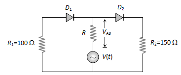
In the circuit given below, V(t) is the sinusoidal voltage source, voltage drop $V_{A B}(t)$ across the resistance R is
- A
- B
- C
Has the same peak value in the positive and negative half cycles
- ✓
Has different peak values during positive and negative half cycle
AnswerCorrect option: D. Has different peak values during positive and negative half cycle
(d) Has different peak values during positive and negative half cycle
View full question & answer→MCQ 551 Mark
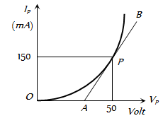
The plate characteristic curve of a diode in space charge limited region is as shown in the figure. The slope of curve at point P is 5.0 mA/V. The static plate resistance of diode will be
- A
111.1$\Omega$
- B
222.2$\Omega$
- ✓
333.3$\Omega$
- D
444.4$\Omega$
AnswerCorrect option: C. 333.3$\Omega$
(c) 333.3$\Omega$
View full question & answer→MCQ 561 Mark
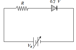
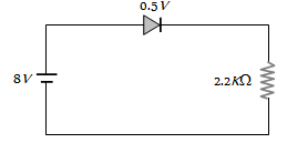
The junction diode in the following circuit requires a minimum current of 1 mA to be above the knee point (0.7 V) of its I-V characteristic curve. The voltage across the diode is independent of current above the knee point. If $V_B=5 V$, then the maximum value of R so that the voltage is above the knee point, will be
- ✓
4.3 k$\Omega$
- B
860 k$\Omega$
- C
4.3$\Omega$
- D
860$\Omega$
AnswerCorrect option: A. 4.3 k$\Omega$
(a) 4.3 k$\Omega$
View full question & answer→MCQ 571 Mark
The value of amplification factor from the following graph will be
MCQ 581 Mark
The mutual characteristic of triode is
Answer(c)

View full question & answer→MCQ 591 Mark
A sinusoidal voltage of peak value 200 volt is connected to a diode and resistor R in the circuit shown so that half wave rectification occurs. If the forward resistance of the diode is negligible compared to R the rms voltage (in volt) across R is approximately
- A
- ✓
- C
$\frac{200}{\sqrt{2}}$
- D
View full question & answer→MCQ 601 Mark
In the following common emitter configuration an NPN transistor with current gain b = 100 is used. The output voltage of the amplifier will be
MCQ 611 Mark
The variation of anode current in a triode corresponding to a change in grid potential at three different values of the plate potential is shown in the diagram. The mutual conductance of the triode is
MCQ 621 Mark
In a negative logic the following wave form corresponds to the
MCQ 631 Mark
The diode used in the circuit shown in the figure has a constant voltage drop of 0.5 V at all currents and a maximum power rating of 100 milliwatts. What should be the value of the resistor R, connected in series with the diode for obtaining maximum current
- A
1.5 $\Omega$
- ✓
5 $\Omega$
- C
6.67 $\Omega$
- D
200 $\Omega$
AnswerCorrect option: B. 5 $\Omega$
(b) 5 $\Omega$
View full question & answer→MCQ 641 Mark
The i-V characteristic of a P-N junction diode is shown below. The approximate dynamic resistance of the P-N junction when a forward bias of 2volt is applied
MCQ 651 Mark
A source voltage of 8V drives the diode in fig. through a current-limiting resistor of 100 ohm. Then the magnitude of the slope load line on the V-I characteristics of the diode is
MCQ 661 Mark
The relation between dynamic plate resistance $\left(r_p\right)$ of a vacuum diode and plate current in the space charge limited region, is
- A
$r_p \propto I_p$
- B
$r_p \propto I_p^{3 / 2}$
- C
$r_p \propto \frac{1}{I_p}$
- ✓
$r_p \propto \frac{1}{\left( I _{ p }\right)^{1 / s }}$
AnswerCorrect option: D. $r_p \propto \frac{1}{\left( I _{ p }\right)^{1 / s }}$
(d) $r_p \propto \frac{1}{\left( I _{ p }\right)^{1 / s }}$
View full question & answer→MCQ 671 Mark
The plate current $i_p$ in a triode valve is given $i_p=K\left(V_p+\mu V_g\right)^{3 / 2}$ where $i_p$ is in milliampere and $V_p$ and $V_g$ are in volt. If $r_p=10^4$ ohm, and $g_m=5 \times 10^{-3} mho$, then for $i_p=8 mA^2$ and $V_p=300$ volt, what is the value of $K$ and grid cut off voltage
- A
$-6 V,(30)^{3 / 2}$
- ✓
$-6 V,(1 / 30)^{3 / 2}$
- C
$+6 V,(30)^{3 / 2}$
- D
$+6 V,(1 / 30)^{3 / 2}$
AnswerCorrect option: B. $-6 V,(1 / 30)^{3 / 2}$
(b) $-6 V,(1 / 30)^{3 / 2}$
View full question & answer→MCQ 681 Mark
The diagram of a logic circuit is given below. The output F of the circuit is represented by
MCQ 691 Mark
The shows two NAND gates followed by a NOR gate. The system is equivalent to the following logic gate
AnswerAND
View full question & answer→MCQ 701 Mark
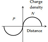
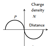
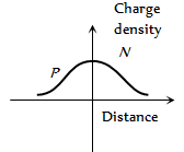
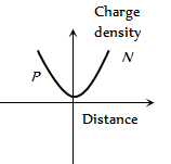
The curve between charge density and distance near P-N junction will be
MCQ 711 Mark
The combination of gates shown below produces
MCQ 721 Mark
In $\text{NPN}$ transistor, $10^{10}$ electrons enters in emitter region in $10^{-6}$ sec. If $2\%$ electrons are lost in base region then collector current and current amplification factor $(b)$ respectively are
- ✓
$1.57 \ mA, 49$
- B
$1.92 \ mA, 70$
- C
$2 \ mA, 25$
- D
$2.25 \ mA, 100$
AnswerCorrect option: A. $1.57 \ mA, 49$
$1.57 \ mA, 49$
View full question & answer→MCQ 731 Mark
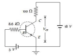
For the transistor circuit shown below, if b = 100, voltage drop between emitter and base is 0.7 V then value of $\mathrm{V}_{\mathrm{CE}}$ will be
View full question & answer→MCQ 741 Mark
In the circuit shown in figure the maximum output voltage $V_0$ is
- A
- ✓
- C
- D
$\frac{5}{\sqrt{2}} V$
View full question & answer→MCQ 751 Mark
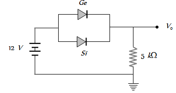
Ge and Si diodes conduct at 0.3 V and 0.7 V respectively. In the following figure if Ge diode connection are reversed, the valve of $V_0$ changes by
View full question & answer→MCQ 761 Mark
The contribution in the total current flowing through a semiconductor due to electrons and holes are $\frac{3}{4}$ and $\frac{1}{4}$ respectively. If the drift velocity of electrons is $\frac{5}{2}$ times that of holes at this temperature, then the ratio of concentration of electrons and holes is
- ✓
$6: 5$
- B
$5: 6$
- C
$3: 2$
- D
$2: 3$
AnswerCorrect option: A. $6: 5$
View full question & answer→MCQ 771 Mark
A potential difference of 2 V is applied between the opposite faces of a Ge crystal plate of area $1 cm^2$ and thickness 0.5 mm . If the concentration of electrons in Ge is $2 \times 10^{19} / m ^3$ and mobilities of electrons and holes are $0.36 \frac{ m ^2}{\text { volt-sec }}$ and $0.14 \frac{ m ^2}{\text { volt-sec }}$ respectively, then the current flowing through the plate will be
View full question & answer→MCQ 781 Mark
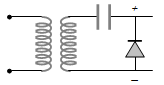
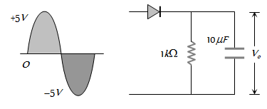
A diode is connected to 220 V (rms) ac in series with a capacitor as shown in figure. The voltage across the capacitor is
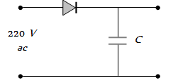
- A
$220\ V$
- B
$110\ V$
- C
$311.1\ V$
- ✓
$\frac{220}{\sqrt 2}V$
AnswerCorrect option: D. $\frac{220}{\sqrt 2}V$
$\frac{220}{\sqrt 2}V$
View full question & answer→MCQ 791 Mark
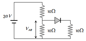
Find $V_{A B}$
View full question & answer→MCQ 801 Mark
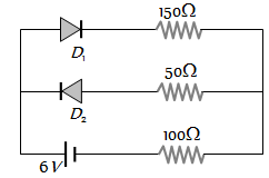
The circuit shown in following figure contains two diode $\mathrm{D}_1$ and $\mathrm{D}_2$ each with a forward resistance of 50 ohms and with infinite backward resistance. If the battery voltage is 6 V, the current through the 100 ohm resistance (in amperes) is
View full question & answer→MCQ 811 Mark
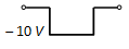
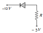
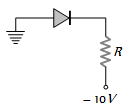
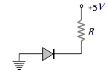
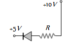
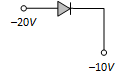
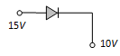
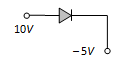
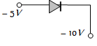
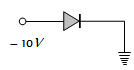
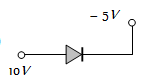
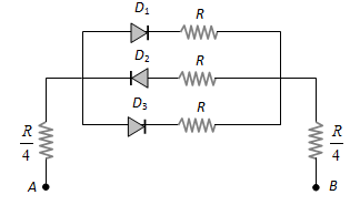
In the following circuits PN-junction diodes $D_1, D_2$ and $D_3$ are ideal for the following potential of A and B, the correct increasing order of resistance between A and B will be
(i) – 10 V, – 5V (ii) – 5V, – 10 V (iii) – 4V, – 12V
View full question & answer→MCQ 821 Mark
The Bohr radius of the fifth electron of phosphorus (atomic number = 15) acting as dopant in silicon (relative dielectric constant = 12) is
MCQ 831 Mark
A transistor is used as an amplifier in CB mode with a load resistance of 5 k W the current gain of amplifier is 0.98 and the input resistance is 70 W, the voltage gain and power gain respectively are
MCQ 841 Mark
The peak voltage in the output of a half-wave diode rectifier fed with a sinusoidal signal without filter is 10 V. The dc component of the output voltage is
- A
$10 / \sqrt{2} V$
- ✓
$10 / p V$
- C
$10 V$
- D
$20 / p V$
AnswerCorrect option: B. $10 / p V$
View full question & answer→MCQ 851 Mark
The grid in a triode valve is used
- A
To increases the thermionic emission
- ✓
To control the plate to cathode current
- C
To reduce the inter-electrode capacity
- D
To keep cathode at constant potential
AnswerCorrect option: B. To control the plate to cathode current
(b) To control the plate to cathode current
View full question & answer→MCQ 861 Mark
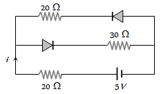
Current in the circuit will be
- A
$\frac{5}{40} A$
- ✓
$\frac{5}{50} A$
- C
$\frac{5}{10} A$
- D
$\frac{5}{20} A$
AnswerCorrect option: B. $\frac{5}{50} A$
$\frac{5}{50} A$
View full question & answer→MCQ 871 Mark
A P-type semiconductor has acceptor levels $57$ meV above the valence band. The maximum wavelength of light required to create a hole is (Planck's constant $h =6.6 \times 10^{-34} J$-s)
AnswerCorrect option: C. $217100 A^0$
(c) $217100 A^0$
View full question & answer→MCQ 881 Mark
In the circuit, if the forward voltage drop for the diode is 0.5V, the current will be
- ✓
$3.4\ mA$
- B
$2\ mA$
- C
$2.5\ mA$
- D
$3\ mA$
AnswerCorrect option: A. $3.4\ mA$
$3.4\ mA$
View full question & answer→MCQ 891 Mark
When a potential difference is applied across, the current passing through
- A
An insulator at 0 K is zero
- B
A semiconductor at 0 K is zero
- C
A P-N diode at 300 K is finite, if it is reverse biased
- ✓
View full question & answer→MCQ 901 Mark
In PN-junction diode the reverse saturation current is $10^{-5} amp$ at $27^{\circ} C$ The forward current for a voltage of 0.2 volt is $\left[\exp (7.62)=2038.6, K=1.4 \times 10^{-23} J / K \right]$
- A
$2037.6 \times 10^{-3} amp$
- B
$203.76 \times 10^{-3} amp$
- ✓
$20.376 \times 10^{-3} amp$
- D
$2.0376 \times 10^3 amp$
AnswerCorrect option: C. $20.376 \times 10^{-3} amp$
(c) $20.376 \times 10^{-3} amp$
View full question & answer→MCQ 911 Mark
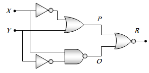
Figure gives a system of logic gates. From the study of truth table it can be found that to produce a high output (1) at R, we must have
MCQ 921 Mark
The following configuration of gate is equivalent to
MCQ 931 Mark
The typical ionisation energy of a donor in silicon is
MCQ 941 Mark
The probability of electrons to be found in the conduction band of an intrinsic semiconductor at a finite temperature
- ✓
Decreases exponentially with increasing band gap
- B
Increases exponentially with increasing band gap
- C
Decreases with increasing temperature
- D
Is independent of the temperature and the band gap
AnswerCorrect option: A. Decreases exponentially with increasing band gap
(a) Decreases exponentially with increasing band gap
View full question & answer→MCQ 951 Mark
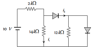
In the following circuit find $\mathrm{I}_1$ and $\mathrm{I}_2$
View full question & answer→MCQ 961 Mark
A silicon speciman is made into a P-type semi-conductor by dopping, on an average, one Indium atom per $5 \times 10^7$ silicon atoms. If the number density of atoms in the silicon specimen is $5 \times 10^{28}$ atoms $/ m ^3$ then the number of acceptor atoms in silicon per cubic centimetre will be
- A
$2.5 \times 10^{30}$ atoms $/ cm ^3$
- B
$1.0 \times 10^{13}$ atoms $/ cm ^3$
- ✓
$1.0 \times 10^{15}$ atoms $/ cm ^3$
- D
$2.5 \times 10^{36}$ atoms $/ cm ^3$
AnswerCorrect option: C. $1.0 \times 10^{15}$ atoms $/ cm ^3$
(c) $1.0 \times 10^{15}$ atoms $/ cm ^3$
View full question & answer→MCQ 971 Mark
Select the correct statement
- ✓
In a full wave rectifier, two diodes work alternately
- B
In a full wave rectifier, two diodes work simultaneously
- C
The efficiency of full wave and half wave rectifiers is same
- D
The full wave rectifier is bi-directional
AnswerCorrect option: A. In a full wave rectifier, two diodes work alternately
(a) In a full wave rectifier, two diodes work alternately
View full question & answer→MCQ 981 Mark
The current in a triode at anode potential $100 V$ and grid potential $– 1.2 V$ is $7.5 mA$. If grid potential is changed to $– 2.2 V,$ the current becomes $5.5 mA.$ the value of trans conductance $(g_m)$ will be
- ✓
$2$ mili mho
- B
$3$ mili mho
- C
$4$ mili mho
- D
$0.2$ mili mho
AnswerCorrect option: A. $2$ mili mho
$2$ mili mho
View full question & answer→MCQ 991 Mark
Plate voltage of a triode is increased from 200 V to 225 V. To maintain the plate current, change in grid voltage from 5V to 5.75 V is needed. The amplification factor is
MCQ 1001 Mark
The plate resistance of a triode is $2.5 \times 10^4 W$ and mutual conductance is $2 \times 10^{-3} \ce{mho}.$ What will be the value of amplification factor
- ✓
$50$
- B
$1.25 \times 10^7$
- C
$75$
- D
$2.25 \times 10^7$
View full question & answer→MCQ 1011 Mark
In a diode valve the cathode temperature must be (f = work function)
- A
High and ∅ should be high
- ✓
- C
- D
View full question & answer→MCQ 1021 Mark
The ripple factor in a half wave rectifier is
MCQ 1031 Mark
The transconductance of a triode amplifier is 2.5 mili mho having plate resistance of 20 KW, amplification 10. Find the load resistance
MCQ 1041 Mark
The slope of plate characteristic of a vacuum diode is $2 \times 10^{-2} mA / V$. The plate resistance of diode will be
- A
$50 \ W$
- ✓
$50 \ kW$
- C
$500 \ kW$
- D
$500 \ kW$
AnswerCorrect option: B. $50 \ kW$
(b) $50 \ kW$
View full question & answer→MCQ 1051 Mark
The amplification factor of a triode is 50. If the grid potential is decreased by 0.20 V, what increase in plate potential will keep the plate current unchanged
MCQ 1061 Mark
The thermionic emission of electron is due to
MCQ 1071 Mark
In a triode valve the amplification factor is $20$ and mutual conductance is $10^{-3} \ce{mho}.$ The plate resistance is
- A
$ 2 \times 10^3 \mathrm{~W} $
- B
$ 4 \times 10^3 \mathrm{~W} $
- ✓
$ 2 \times 10^4 \mathrm{~W} $
- D
$ 2 \times 10^4 \mathrm{~W}$
AnswerCorrect option: C. $ 2 \times 10^4 \mathrm{~W} $
$ 2 \times 10^4 \mathrm{~W} $
View full question & answer→MCQ 1081 Mark
The voltage gain of a triode depends upon
MCQ 1091 Mark
The electrical circuits used to get smooth d.c. output from a rectifier circuit is called
MCQ 1101 Mark
For a given triode μ = 20. The load resistance is 1.5 times the anode resistance. The maximum gain will be
MCQ 1111 Mark
View full question & answer→MCQ 1121 Mark
Plate resistance of two triode valves is 2 KW and 4 KW, amplification factor of each of the valves is 40. The ratio of voltage amplification, when used with 4 KW load resistance, will be
- A
$10$
- B
$\frac{4}{3}$
- ✓
$\frac{3}{4}$
- D
$\frac{16}{3}$
AnswerCorrect option: C. $\frac{3}{4}$
$\frac{3}{4}$
View full question & answer→MCQ 1131 Mark
In a diode valve, the state of saturation can be obtained easily by
- A
High plate voltage and high filament current
- ✓
Low filament current and high plate voltage
- C
Low plate voltage and high cathode temperature
- D
High filament current and high plate voltage
AnswerCorrect option: B. Low filament current and high plate voltage
Low filament current and high plate voltage
View full question & answer→MCQ 1141 Mark
When plate voltage in diode valve is increased from 100 volt to 150 volt then plate current increases from 7.5 mA to 12 mA. The dynamic plastic resistance will be
MCQ 1151 Mark
A 2V battery is connected across the points A and B as shown in the figure given below. Assuming that the resistance of each diode is zero in forward bias and infinity in reverse bias, the current supplied by the battery when its positive terminal is connected to A is
MCQ 1161 Mark
Which one is correct relation for thermionic emission
- A
$J=A T^{1 / 2} e^{-\emptyset / k T}$
- ✓
$J = AT ^2 e ^{-\varnothing / kT }$
- C
$J=A T^{3 / 2} e^{-\emptyset / k T}$
- D
$J=A T^2 e^{-\emptyset / 2 k T}$
AnswerCorrect option: B. $J = AT ^2 e ^{-\varnothing / kT }$
(b) $J = AT ^2 e ^{-\varnothing / kT }$
View full question & answer→MCQ 1171 Mark
Following is the relation between current and charge $I = AT ^2 e ^{ qt / v _{ L }}$ then value of $V _{ L }$ will be
- A
$\frac{ V }{ kT }$
- B
$\frac{ kV }{ T }$
- ✓
$\frac{ kT }{ v }$
- D
$\frac{ VT }{ k }$
AnswerCorrect option: C. $\frac{ kT }{ v }$
(c) $\frac{ kT }{ v }$
View full question & answer→MCQ 1181 Mark
Correct relation for triode is
AnswerCorrect option: A. $\mu=g_m \times r_p$
(a) $\mu=g_m \times r_p$
View full question & answer→MCQ 1191 Mark
Coating of strontium oxide on Tungsten cathode in a valve is good for thermionic emission because
- ✓
- B
- C
Conductivity of cathode increases
- D
Cathode can be heated to high temperature
View full question & answer→MCQ 1201 Mark
The value of plate current in the given circuit diagram will be
MCQ 1211 Mark
Before the saturation state of a diode at the plate voltages of 400 V and 200 V respectively the currents are $\mathrm{i}_1$ and $\mathrm{i}_2$ respectively. The ratio $i_1 / i_2$ will be
- A
$\sqrt{2/4}$
- B
$2\sqrt2$
- ✓
$2$
- D
$1/2$
View full question & answer→MCQ 1221 Mark
The introduction of a grid in a triode valve affects plate current by
- A
Making the thermionic emission easier at low temperature
- B
Releasing more electrons from the plate
- C
By increasing plate voltage
- ✓
By neutralising space charge
AnswerCorrect option: D. By neutralising space charge
By neutralising space charge
View full question & answer→MCQ 1231 Mark
With a change of load resistance of a triode, used as an amplifier, from 50 kilo ohms to 100 kilo ohms, its voltage amplification changes from 25 to 30. Plate resistance of the triode is
MCQ 1241 Mark
The unit of mutual conductance of a triode valve is
MCQ 1251 Mark
The triode constant is out of the following
MCQ 1261 Mark
For a triode, at $v _{ g }=-1$ volt, the following observations were taken $v _{ p }=75 V, I _{ p }=2 mA, V _{ p }=100 V, I _{ p }=4 mA$. The value of plate resistance will be
- A
$25$ kW
- B
$20.8$ kW
- ✓
$12.5$ kW
- D
$100$ kW
AnswerCorrect option: C. $12.5$ kW
(c) $12.5$ kW
View full question & answer→MCQ 1271 Mark
If the amplification factor of a triode (m) is 22 and its plate resistance is 6600 ohm, then the mutual conductance of this valve is mho is
- ✓
$\frac{1}{300}$
- B
$25 \times 10^{-2}$
- C
$2.5 \times 10^{-2}$
- D
$0.25 \times 10^{-2}$
AnswerCorrect option: A. $\frac{1}{300}$
(a) $\frac{1}{300}$
View full question & answer→MCQ 1281 Mark
In the circuit of a triode valve, there is no change in the plate current, when the plate potential is increased from 200 volt to 220 volt and the grid potential is decreased from – 0.5 volt to –1.3 volt. The amplification factor of this valve is
MCQ 1291 Mark
$14 \times 10^{15}$ electrons reach the anode per second. If the power consumed is 448 milliwatts, then the plate (anode) voltage is
View full question & answer→MCQ 1301 Mark
The slope of plate characteristic of a vacuum tube diode for certain operating point on the curve is $10^{-3} \frac{ mA }{ V }$. The plate resistance of the diode and its nature respectively
- A
$100$ kilo-ohms static
- ✓
$1000$ kilo-ohms static
- C
$1000$ kilo-ohms dynamic
- D
$100$ kilo-ohms dynamic
AnswerCorrect option: B. $1000$ kilo-ohms static
(b) $1000$ kilo-ohms static
View full question & answer→MCQ 1311 Mark
The amplification factor of a triode valve is 15. If the grid voltage is changed by 0.3 volt the change in plate voltage in order to keep the plate current constant (in volt) is
MCQ 1321 Mark
- A
If the grid voltage is zero then plate current will be zero
- B
If the temperature of filament is doubled, then the thermionic current will also be doubled
- ✓
If the temperature of filament is doubled, then the thermionic current will nearly be four times
- D
At a definite grid voltage the plate current varies with plate voltage according to Ohm’s law
AnswerCorrect option: C. If the temperature of filament is doubled, then the thermionic current will nearly be four times
If the temperature of filament is doubled, then the thermionic current will nearly be four times
View full question & answer→MCQ 1331 Mark
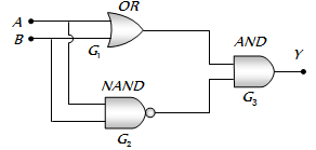
The combination of the gates shown in the figure below produces
MCQ 1341 Mark
To get an output 1 from the circuit shown in the figure, the input must be
MCQ 1351 Mark
In a triode amplifier, the value of maximum gain is equal to
- A
Half the amplification factor
- ✓
- C
Twice the amplification factor
- D
View full question & answer→MCQ 1361 Mark
In an experiment, the saturation in the plate current in a diode is observed at 240V. But a student still wants to increase the plate current. It can be done, if
- A
The plate voltage is increased further
- B
The plate voltage is decreased
- C
The filament current is decreased
- ✓
The filament current is increased
AnswerCorrect option: D. The filament current is increased
The filament current is increased
View full question & answer→MCQ 1371 Mark
The amplification produced by a triode is due to the action of
MCQ 1381 Mark
For a triode $r_P=10$ kilo ohm and $g_m=3$ milli mho. If the load resistance is double of plate resistance, then the value of voltage gain will be(a) 10(b) 20(c) 15(d) 30
View full question & answer→MCQ 1391 Mark
The amplification factor of a triode is 20. If the grid potential is reduced by 0.2 volt then to keep the plate current constant its plate voltage is to be increased by
MCQ 1401 Mark
In a triode amplifier, $\mu=25, r_P=40$ kilo ohm and load resistance $R_L=10$ kilo ohm. If the input signal voltage is 0.5 volt, then output signal voltage will be
- A
$1.25$ volt
- B
$5$ volt
- ✓
$2.5$ volt
- D
$10$ volt
AnswerCorrect option: C. $2.5$ volt
(c) $2.5$ volt
View full question & answer→MCQ 1411 Mark
The amplification factor of a triode is 20 and trans-conductance is 3 milli mho and load resistance $3 \times 10^4 \Omega$, then the voltage gain is
View full question & answer→MCQ 1421 Mark
If $\mathrm{R}_{\mathrm{p}}=7 \mathrm{~K} \Omega, \mathrm{gm}=2.5$ millimho, then on increasing plate voltage by 50 V, how much the grid voltage is changed so that plate current remains the same
View full question & answer→MCQ 1431 Mark
For a given plate-voltage, the plate current in a triode is maximum when the potential of
- A
The grid is positive and plate is negative
- ✓
The grid is positive and plate is positive
- C
The grid is zero and plate is positive
- D
The grid is negative and plate is positive
AnswerCorrect option: B. The grid is positive and plate is positive
The grid is positive and plate is positive
View full question & answer→MCQ 1441 Mark
In an amplifier the load resistance $\mathrm{R}_{\mathrm{L}}$ is equal to the plate resistance ($\mathrm {r_p}$). The voltage amplification is equal to
View full question & answer→MCQ 1451 Mark
The grid voltage of any triode valve is changed from –1 volt to – 3 volt and the mutual conductance is $3 \times 10^{-4}$ mho. The change in plate circuit current will be
View full question & answer→MCQ 1461 Mark
In diode, when there is saturation current, the plate resistance $(r_p)$ is
View full question & answer→MCQ 1471 Mark
Number of secondary electrons emitted per number of primary electrons depends on
- A
- B
Frequency of primary electrons
- ✓
- D
View full question & answer→MCQ 1481 Mark
Thermionic emission from a heated filament varies with its temperature $T$ as
- A
$T ^{-1}$
- B
$T$
- ✓
$T ^2$
- D
$T^{3 / 2}$
AnswerCorrect option: C. $T ^2$
(c) $T ^2$
View full question & answer→MCQ 1491 Mark
Which of the following logic gate is an universal gate
MCQ 1501 Mark
Sum of the two binary numbers $(10000)_2$ and $(11011)_2$ is
- ✓
$(111101)_2$
- B
$(1111111)_2$
- C
$(101111)_2$
- D
$(111001)_2$
AnswerCorrect option: A. $(111101)_2$
(a) $(111101)_2$
View full question & answer→MCQ 1511 Mark
Which gates is represented by this figure
MCQ 1521 Mark
The output of OR gate is 1
- A
- ✓
If either or both inputs are 1
- C
- D
AnswerCorrect option: B. If either or both inputs are 1
If either or both inputs are 1
View full question & answer→MCQ 1531 Mark
Which logic gate is represented by the following combination of logic gates
MCQ 1541 Mark
A gate in which all the inputs must be low to get a high output is called
MCQ 1551 Mark
The output of a NAND gate is 0
- A
- B
If one input is 0 and the other input is 1
- ✓
- D
Either if both inputs are 1 or if one of the inputs is 1 and the other 0
View full question & answer→MCQ 1561 Mark
In the CB mode of a transistor, when the collector voltage is changed by 0.5 volt. The collector current changes by 0.05 mA. The output resistance will be
MCQ 1571 Mark
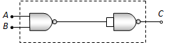
Which logic gate is represented by following diagram
MCQ 1581 Mark
This symbol represents
MCQ 1591 Mark
The Boolean equation of NOR gate is
AnswerCorrect option: B. $C =\overline{ A + B }$
(b) $C=\overline{A+B}$
View full question & answer→MCQ 1601 Mark
If A and B are two inputs in AND gate, then AND gate has an output of 1 when the values of A and B are
MCQ 1611 Mark
The given truth table is of
MCQ 1621 Mark
Which represents NAND gate
MCQ 1631 Mark
Which of the following gates will have an output of 1(a)
MCQ 1641 Mark
How many NAND gates are used to form an AND gate
MCQ 1651 Mark
A gate has the following truth table
| P |
1 |
1 |
0 |
0 |
| Q |
1 |
0 |
1 |
0 |
| R |
1 |
0 |
0 |
0 |
The gate is
MCQ 1661 Mark
A logic gate is an electronic circuit which
- ✓
- B
Allows electrons flow only in one direction
- C
- D
Alternates between 0 and 1 values
View full question & answer→MCQ 1671 Mark
The logic behind ‘NOR’ gate is that it gives
- ✓
High output when both the inputs are low
- B
Low output when both the inputs are low
- C
High output when both the inputs are high
- D
AnswerCorrect option: A. High output when both the inputs are low
High output when both the inputs are low
View full question & answer→MCQ 1681 Mark
Boolean algebra is essentially based on
MCQ 1691 Mark
The truth table shown in figure is for
| A |
0 |
0 |
1 |
1 |
| B |
0 |
1 |
0 |
1 |
| y |
1 |
0 |
0 |
1 |
MCQ 1701 Mark
Given below are four logic gate symbol (figure). Those for OR, NOR and NAND are respectively
MCQ 1711 Mark
In a transistor in CE configuration, the ratio of power gain to voltage gain is
MCQ 1721 Mark
NPN transistor are preferred to PNP transistor because they have
- A
- B
- C
Capability of handing large power
- ✓
Electrons having high mobility than holes
AnswerCorrect option: D. Electrons having high mobility than holes
Electrons having high mobility than holes
View full question & answer→MCQ 1731 Mark
In NPN transistor the collector current is 10 mA. If 90% of electrons emitted reach the collector, then
- A
Emitter current will be 9 mA
- ✓
Emitter current will be 11.1 mA
- C
Base current will be 0.1 mA
- D
Base current will be 0.01 mA
AnswerCorrect option: B. Emitter current will be 11.1 mA
Emitter current will be 11.1 mA
View full question & answer→MCQ 1741 Mark
Consider an NPN transistor amplifier in common-emitter configuration. The current gain of the transistor is 100. If the collector current changes by 1 mA, what will be the change in emitter current
MCQ 1751 Mark
While a collector to emitter voltage is constant in a transistor, the collector current changes by $8.2 mA$ when the emitter current changes by $8.3 mA.$ The value of forward current ratio $h_{fe}$ is
View full question & answer→MCQ 1761 Mark
Which of the following is used to produce radio waves of constant amplitude
MCQ 1771 Mark
In an $\ce{NPN}$ transistor circuit, the collector current is $10 \ mA.$ If $90\%$ of the electrons emitted reach the collector, the emitter current $(i_E)$ and base current $(i_B)$ are given by
- A
$ \mathrm{i}_{\mathrm{E}}=-1 \mathrm{~mA}, \mathrm{i}_{\mathrm{B}}=9 \mathrm{~mA} $
- B
$ \mathrm{i}_{\mathrm{E}}=9 \mathrm{~mA}, \mathrm{i}_{\mathrm{B}}=-1 \mathrm{~mA} $
- C
$ \mathrm{i}_{\mathrm{E}}=1 \mathrm{~mA}, \mathrm{i}_{\mathrm{B}}=11 \mathrm{~mA} $
- ✓
$ \mathrm{i}_{\mathrm{E}}=11 \mathrm{~mA}, \mathrm{i}_{\mathrm{B}}=1 \mathrm{~mA}$
AnswerCorrect option: D. $ \mathrm{i}_{\mathrm{E}}=11 \mathrm{~mA}, \mathrm{i}_{\mathrm{B}}=1 \mathrm{~mA}$
$ \mathrm{i}_{\mathrm{E}}=11 \mathrm{~mA}, \mathrm{i}_{\mathrm{B}}=1 \mathrm{~mA}$
View full question & answer→MCQ 1781 Mark
If $l_1, l_2, l_3$ are the lengths of the emitter, base and collector of a transistor then
- A
$l_1=l_2=l_3$
- B
$l_3 < l_2 < l_1$
- C
$l_3 < l_1 < l_2$
- ✓
$l_3 > l_1 > l_2$
AnswerCorrect option: D. $l_3 > l_1 > l_2$
$l_3 > l_1 > l_2$
View full question & answer→MCQ 1791 Mark
When NPN transistor is used as an amplifier
- A
Electrons move from base to emitter
- ✓
Electrons move from emitter to base
- C
Electrons moves from base to emitter
- D
Holes moves from base to emitter
AnswerCorrect option: B. Electrons move from emitter to base
Electrons move from emitter to base
View full question & answer→MCQ 1801 Mark
The relation between $a$ and $b$ parameters of current gains for a transistors is given by
- A
$\alpha=\frac{\beta}{1-\beta}$
- ✓
$\alpha=\frac{\beta}{1+\beta}$
- C
$\alpha=\frac{1-\beta}{\beta}$
- D
$\alpha=\frac{1+\beta}{\beta}$
AnswerCorrect option: B. $\alpha=\frac{\beta}{1+\beta}$
$\alpha=\frac{\beta}{1+\beta}$
View full question & answer→MCQ 1811 Mark
For a transistor, in a common emitter arrangement, the alternating current gain $b$ is given by
- ✓
$\beta=\left(\frac{\Delta I }{\Delta I _{ B }}\right)_{ vc }$
- B
$\beta=$ $\left(\frac{\Delta I _{ E }}{\Delta I _{ C }}\right)_{ v c }$
- C
$\beta=\left(\frac{\Delta I _{ c }}{\Delta I _{ E }}\right)_{ v c }$
- D
$\beta=\left(\frac{\Delta II _{ E }}{\Delta IC _{ C }}\right)_{ v c }$
AnswerCorrect option: A. $\beta=\left(\frac{\Delta I }{\Delta I _{ B }}\right)_{ vc }$
$\beta=\left(\frac{\Delta I _{ C }}{\Delta I _{ B }}\right)_{ vc }$
View full question & answer→MCQ 1821 Mark
Which of these is unipolar transistor
MCQ 1831 Mark
In a transistor configuration b-parameter is
AnswerCorrect option: B. $\frac{l_{ c }}{1_b}$
$\frac{l_{ c }}{1_b}$
View full question & answer→MCQ 1841 Mark
In a transistor, a change of 8.0 mA in the emitter current produces a change of 7.8 mA in the collector current. What change in the base current is necessary to produce the same change in the collector current
MCQ 1851 Mark
In a transistor circuit shown here the base current is 35 mA. The value of the resistor $\mathrm{R}_{\mathrm{b}}$ is
View full question & answer→MCQ 1861 Mark
In case of NPN-transistors the collector current is always less than the emitter current because
- A
Collector side is reverse biased and emitter side is forward biased
- ✓
After electrons are lost in the base and only remaining ones reach the collector
- C
Collector side is forward biased and emitter side is reverse biased
- D
Collector being reverse biased attracts less electrons
AnswerCorrect option: B. After electrons are lost in the base and only remaining ones reach the collector
After electrons are lost in the base and only remaining ones reach the collector
View full question & answer→MCQ 1871 Mark
In a common base amplifier circuit, calculate the change in base current if that in the emitter current is 2 mA and a = 0.98
MCQ 1881 Mark
For a transistor, the current amplification factor is 0.8. The transistor is connected in common emitter configuration. The change in the collector current when the base current changes by 6 mA is
MCQ 1891 Mark
The part of a transistor which is heavily doped to produce a large number of majority carriers, is
MCQ 1901 Mark
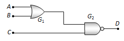
For the given combination of gates, if the logic states of inputs A, B, C are as follows A = B = C = 0 and A = B = 1, C = 0 then the logic states of output D are
MCQ 1911 Mark
An NPN-transistor circuit is arranged as shown in figure. It is
- A
A common base amplifier circuit
- ✓
A common emitter amplifier circuit
- C
A common collector amplifier circuit
- D
AnswerCorrect option: B. A common emitter amplifier circuit
A common emitter amplifier circuit
View full question & answer→MCQ 1921 Mark
The most commonly used material for making transistor is
MCQ 1931 Mark
The combination of ‘NAND’ gates shown here under (figure) are equivalent to
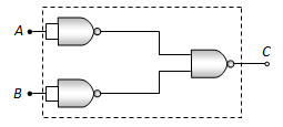
- ✓
An OR gate and an AND gate respectively
- B
An AND gate and a NOT gate respectively
- C
An AND gate and an OR gate respectively
- D
An OR gate and a NOT gate respectively.
AnswerCorrect option: A. An OR gate and an AND gate respectively
An OR gate and an AND gate respectively
View full question & answer→MCQ 1941 Mark
The symbol given in figure represents
- ✓
- B
- C
Forward biased PN junction diode
- D
Reverse biased NP junction diode
View full question & answer→MCQ 1951 Mark
A common emitter amplifier is designed with NPN transistor (a = 0.99). The input impedance is 1 KW and load is 10 KW. The voltage gain will be
MCQ 1961 Mark
Given below are symbols for some logic gates
The XOR gate and NOR gate respectively are
MCQ 1971 Mark
In a PNP transistor the base is the N-region. Its width relative to the P-region is
MCQ 1981 Mark
A transistor is used in common emitter mode as an amplifier. Then
- A
The base-emitter junction is forward biased
- B
The base-emitter junction is reverse biased
- C
The input signal is connected in series with the voltage applied to the base-emitter junction
- ✓
View full question & answer→MCQ 1991 Mark
For a transistor the parameter b = 99. The value of the parameter a is
MCQ 2001 Mark
The transfer ratio of a transistor is 50. The input resistance of the transistor when used in the common-emitter configuration is 1 KW. The peak value for an A.C input voltage of 0.01 V peak is
MCQ 2011 Mark
The transistors provide good power amplification when they are used in
- A
Common collector configuration
- ✓
Common emitter configuration
- C
Common base configuration
- D
AnswerCorrect option: B. Common emitter configuration
Common emitter configuration
View full question & answer→MCQ 2021 Mark
Least doped region in a transistor
- A
Either emitter or collector
- ✓
- C
- D
View full question & answer→MCQ 2031 Mark
In a common emitter transistor, the current gain is 80. What is the change in collector current, when the change in base current is 250 mA
MCQ 2041 Mark
Symbolic representation of photodiode is
MCQ 2051 Mark
In P-N junction, the barrier potential offers resistance to
- ✓
Free electrons in N region and holes in P region
- B
Free electrons in P region and holes in N region
- C
Only free electrons in N region
- D
AnswerCorrect option: A. Free electrons in N region and holes in P region
Free electrons in N region and holes in P region
View full question & answer→MCQ 2061 Mark
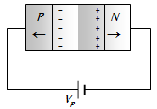
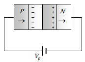
A semiconductor X is made by doping a germanium crystal with arsenic (Z = 33). A second semiconductor Y is made by doping germanium with indium (Z = 49). The two are joined end to end and connected to a battery as shown. Which of the following statements is correct
- A
X is P-type, Y is N-type and the junction is forward biased
- B
X is N-type, Y is P-type and the junction is forward biased
- C
X is P-type, Y is N-type and the junction is reverse biased
- ✓
X is N-type, Y is P-type and the junction is reverse biased
AnswerCorrect option: D. X is N-type, Y is P-type and the junction is reverse biased
X is N-type, Y is P-type and the junction is reverse biased
View full question & answer→MCQ 2071 Mark
The width of forbidden gap in silicon crystal is 1.1 eV. When the crystal is converted in to a N-type semiconductor the distance of Fermi level from conduction band is
MCQ 2081 Mark
View full question & answer→MCQ 2091 Mark
In a PNP transistor working as a common-base amplifier, current gain is 0.96 and emitter current is 7.2 mA. The base current is
MCQ 2101 Mark
For a common base configuration of PNP transistor $\frac{1_{ C }}{1_{ E }}=0.98$ then maximum current gain in common emitter configuration will be
View full question & answer→MCQ 2111 Mark
If $a = 0.98$ and current through emitter $i_e= 20 \ mA$, the value of $b$ is
View full question & answer→MCQ 2121 Mark
Which of the following is true
- A
Common base transistor is commonly used because current gain is maximum
- ✓
Common emitter is commonly used because current gain is maximum
- C
Common collector is commonly used because current gain is maximum
- D
Common emitter is the least used transistor
AnswerCorrect option: B. Common emitter is commonly used because current gain is maximum
Common emitter is commonly used because current gain is maximum
View full question & answer→MCQ 2131 Mark
In the case of constants a and b of a transistor
MCQ 2141 Mark
A NPN transistor conducts when
- A
Both collector and emitter are positive with respect to the base
- ✓
Collector is positive and emitter is negative with respect to the base
- C
+ Collector is positive and emitter is at same potential as the base
- D
Both collector and emitter are negative with respect to the base
AnswerCorrect option: B. Collector is positive and emitter is negative with respect to the base
Collector is positive and emitter is negative with respect to the base
View full question & answer→MCQ 2151 Mark
In an NPN transistor the collector current is 24 mA. If 80% of electrons reach collector its base current in mA is
MCQ 2161 Mark
The emitter-base junction of a transistor is …… biased while the collector-base junction is ……. biased
MCQ 2171 Mark
An oscillator is nothing but an amplifier with
MCQ 2181 Mark
The phase difference between input and output voltages of a $\ce{CE}$ circuit is
- A
$ 0^{\circ} $
- B
$ 90^{\circ} $
- ✓
$ 180^{\circ} $
- D
$ 270^{\circ}$
AnswerCorrect option: C. $ 180^{\circ} $
$ 180^{\circ}$
View full question & answer→MCQ 2191 Mark
When NPN transistor is used as an amplifier
- ✓
Electrons move from base to collector
- B
Holes move from emitter to base
- C
Electrons move from collector to base
- D
Holes move from base to emitter
AnswerCorrect option: A. Electrons move from base to collector
Electrons move from base to collector
View full question & answer→MCQ 2201 Mark
In a full wave rectifiers, input ac current has a frequency ‘n’. The output frequency of current is
MCQ 2211 Mark
If a full wave rectifier circuit is operating from 50 Hz mains, the fundamental frequency in the ripple will be
MCQ 2221 Mark
The current through an ideal PN-junction shown in the following circuit diagram will be
MCQ 2231 Mark
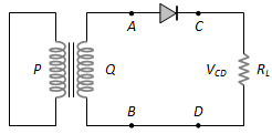
In the diagram, the input is across the terminals A and C and the output is across the terminals B and D, then the output is
MCQ 2241 Mark
The depletion layer in silicon diode is $1 \ mm$ wide and the knee potential is $0.6 V,$ then the electric field in the depletion layer will be
- A
- B
$ 0.6\ \mathrm{Vm}^{-1} $
- ✓
$ 6 \times 10^4 \mathrm{~V} / \mathrm{m} $
- D
$ 6 \times 10^5 \mathrm{~V} / \mathrm{m}$
AnswerCorrect option: C. $ 6 \times 10^4 \mathrm{~V} / \mathrm{m} $
$ 6 \times 10^5 \mathrm{~V} / \mathrm{m}$
View full question & answer→MCQ 2251 Mark
Which is the wrong statement in following sentences? A device in which P and N-type semiconductors are used is more useful then a vacuum type because
- A
Power is not necessary to heat the filament
- B
- C
Very less heat is produced in it
- ✓
Its efficiency is high due to a high voltage across the junction
AnswerCorrect option: D. Its efficiency is high due to a high voltage across the junction
Its efficiency is high due to a high voltage across the junction
View full question & answer→MCQ 2261 Mark
To make a PN junction conducting
- ✓
The value of forward bias should be more than the barrier potential
- B
The value of forward bias should be less than the barrier potential
- C
The value of reverse bias should be more than the barrier potential
- D
The value of reverse bias should be less than the barrier potential
AnswerCorrect option: A. The value of forward bias should be more than the barrier potential
The value of forward bias should be more than the barrier potential
View full question & answer→MCQ 2271 Mark
If no external voltage is applied across P-N junction, there would be
- A
No electric field across the junction
- ✓
An electric field pointing from N-type to P-type side across the junction
- C
An electric field pointing from P-type to N-type side across the junction
- D
A temporary electric field during formation of P-N junction that would subsequently disappear
AnswerCorrect option: B. An electric field pointing from N-type to P-type side across the junction
An electric field pointing from N-type to P-type side across the junction
View full question & answer→MCQ 2281 Mark
A potential barrier of 0.50 V exists across a P-N junction. If the depletion region is $5.0 \times 10^{-7} V / m$ wide, the intensity of the electric field in this region is
- ✓
$1.0 \times 10^6 V / m$
- B
$1.0 \times 10^5 V / m$
- C
$2.0 \times 10^5 V / m$
- D
$2.0 \times 10^6 V / m$
AnswerCorrect option: A. $1.0 \times 10^6 V / m$
$1.0 \times 10^6 V / m$
View full question & answer→MCQ 2291 Mark
No bias is applied to a P-N junction, then the current
- A
Is zero because the number of charge carriers flowing on both sides is same
- ✓
Is zero because the charge carriers do not move
- C
- D
AnswerCorrect option: B. Is zero because the charge carriers do not move
Is zero because the charge carriers do not move
View full question & answer→MCQ 2301 Mark
Which one of the following statements is not correct
- A
A diode does not obey Ohm's law
- B
A PN junction diode symbol shows an arrow identifying the direction of current (forward) flow
- ✓
An ideal diode is an open switch
- D
An ideal diode is an ideal one way conductor
AnswerCorrect option: C. An ideal diode is an open switch
An ideal diode is an open switch
View full question & answer→MCQ 2311 Mark
The correct symbol for zener diode is
MCQ 2321 Mark
Consider the following statements A and B and identify the correct choice of the given answers
(A) A zener diode is always connected in reverse bias
(B) The potential barrier of a PN junction lies between 0.1 to 0.3 V approximately
- A
- B
- ✓
A is correct but B is wrong
- D
A is wrong but B is correct
AnswerCorrect option: C. A is correct but B is wrong
A is correct but B is wrong
View full question & answer→MCQ 2331 Mark
Zener breakdown takes place if
MCQ 2341 Mark
The diode shown in the circuit is a silicon diode. The potential difference between the points A and B will be
MCQ 2351 Mark
In order to forward bias a PN junction, the negative terminal of battery is connected to
MCQ 2361 Mark
Select the correct statement
- ✓
In a full wave rectifier, two diodes work alternately
- B
In a full wave rectifier, two diodes work simultaneously
- C
The efficiency of full wave and half wave rectifiers is same
- D
The full wave rectifier is bi-directional.
AnswerCorrect option: A. In a full wave rectifier, two diodes work alternately
In a full wave rectifier, two diodes work alternately
View full question & answer→MCQ 2371 Mark
Serious draw back of the semiconductor device is
- ✓
They cannot be used with high voltage
- B
They pollute the environment
- C
- D
They do not last for long time
AnswerCorrect option: A. They cannot be used with high voltage
They cannot be used with high voltage
View full question & answer→MCQ 2381 Mark
The maximum efficiency of full wave rectifier is
MCQ 2391 Mark
Which is the correct diagram of a half-wave rectifier(a)
MCQ 2401 Mark
In a PN junction photo cell, the value of photo-electromotive force produced by monochromatic light is proportional to
- A
The voltage applied at the PN junction
- B
The barrier voltage at the PN junction
- ✓
The intensity of the light falling on the cell
- D
The frequency of the light falling on the cell
AnswerCorrect option: C. The intensity of the light falling on the cell
The intensity of the light falling on the cell
View full question & answer→MCQ 2411 Mark
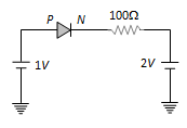
Of the diodes shown in the following diagrams, which one is reverse biased
MCQ 2421 Mark
View full question & answer→MCQ 2431 Mark
Barrier potential of a P-N junction diode does not depend on
MCQ 2441 Mark
In the middle of the depletion layer of a reverse-biased PN junction, the
- A
- B
- C
- ✓
Electric field is maximum
AnswerCorrect option: D. Electric field is maximum
Electric field is maximum
View full question & answer→MCQ 2451 Mark
For the given circuit of PN-junction diode, which of the following statement is correct
- ✓
In forward biasing the voltage across R is V
- B
In forward biasing the voltage across R is 2V
- C
In reverse biasing the voltage across R is V
- D
In reverse biasing the voltage across R is 2V
AnswerCorrect option: A. In forward biasing the voltage across R is V
In forward biasing the voltage across R is V
View full question & answer→MCQ 2461 Mark
- A
P and N both are at same potential
- ✓
High potential at N side and low potential at P side
- C
High potential at P side and low potential at N side
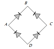
- D
Low potential at N side and zero potential at P side
AnswerCorrect option: B. High potential at N side and low potential at P side
High potential at N side and low potential at P side
View full question & answer→MCQ 2471 Mark
The dominant mechanisms for motion of charge carriers in forward and reverse biased silicon P-N junctions are
- A
Drift in forward bias, diffusion in reverse bias
- ✓
Diffusion in forward bias, drift in reverse bias
- C
Diffusion in both forward and reverse bias
- D
Drift in both forward and reverse bias
AnswerCorrect option: B. Diffusion in forward bias, drift in reverse bias
Diffusion in forward bias, drift in reverse bias
View full question & answer→MCQ 2481 Mark
If the two ends P and N of a P-N diode junction are joined by a wire
- ✓
There will not be a steady current in the circuit
- B
There will be a steady current from N side to P side
- C
There will be a steady current from P side to N side
- D
There may not be a current depending upon the resistance of the connecting wire
AnswerCorrect option: A. There will not be a steady current in the circuit
There will not be a steady current in the circuit
View full question & answer→MCQ 2491 Mark
When the P end of P-N junction is connected to the negative terminal of the battery and the N end to the positive terminal of the battery, then the P-N junction behaves like
MCQ 2501 Mark
View full question & answer→MCQ 2511 Mark
The potential barrier, in the depletion layer, is due to
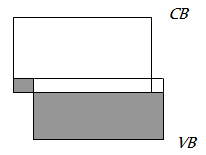
MCQ 2521 Mark
When forward bias is applied to a $P - N$ junction, then what happens to the potential barrier $V _{ B }$, and the width of charge depleted region $x$
- A
$V_B$ increases, $x$ decreases
- B
$V _{ B }$ decreases, x increases
- C
$V_B$ increases, $x$ increases
- ✓
$V_B$ decreases, $x$ decreases
AnswerCorrect option: D. $V_B$ decreases, $x$ decreases
$V_B$ decreases, $x$ decreases
View full question & answer→MCQ 2531 Mark
Zener breakdown in a semi-conductor diode occurs when
- A
Forward current exceeds certain value
- ✓
Reverse bias exceeds certain value
- C
Forward bias exceeds certain value
- D
Potential barrier is reduced to zero
AnswerCorrect option: B. Reverse bias exceeds certain value
Reverse bias exceeds certain value
View full question & answer→MCQ 2541 Mark
Which is reverse biased diode
MCQ 2551 Mark
Avalanche breakdown is due to
- ✓
Collision of minority charge carrier
- B
Increase in depletion layer thickness
- C
Decrease in depletion layer thickness
- D
AnswerCorrect option: A. Collision of minority charge carrier
Collision of minority charge carrier
View full question & answer→MCQ 2561 Mark
In comparison to a half wave rectifier, the full wave rectifier gives lower
MCQ 2571 Mark
Consider the following statements A and B and identify the correct choice of the given answers
A : The width of the depletion layer in a P-N junction diode increases in forwards bias
B : In an intrinsic semiconductor the fermi energy level is exactly in the middle of the forbidden gap
MCQ 2581 Mark
Which of the following statements is not true
- A
The resistance of intrinsic semiconductors decrease with increase of temperature
- B
Doping pure Si with trivalent impurities give P-type semiconductors
- ✓
The majority carriers in N-type semiconductors are holes
- D
A PN-junction can act as a semiconductor diode
AnswerCorrect option: C. The majority carriers in N-type semiconductors are holes
The majority carriers in N-type semiconductors are holes
View full question & answer→MCQ 2591 Mark
The resistance of a reverse biased P-N junction diode is about
- A
$1$ ohm
- B
$10^2 ohm$
- C
$10^3 ohm$
- ✓
$10^6 ohm$
AnswerCorrect option: D. $10^6 ohm$
$10^6 ohm$
View full question & answer→MCQ 2601 Mark
In a PN-junction diode not connected to any circuit
- A
The potential is the same everywhere
- B
The P-type is a higher potential than the N-type side
- ✓
There is an electric field at the junction directed from the N- type side to the P- type side
- D
There is an electric field at the junction directed from the P-type side to the N-type side
AnswerCorrect option: C. There is an electric field at the junction directed from the N- type side to the P- type side
There is an electric field at the junction directed from the N- type side to the P- type side
View full question & answer→MCQ 2611 Mark
The cause of the potential barrier in a P-N diode is
- A
Depletion of positive charges near the junction
- B
Concentration of positive charges near the junction
- C
Depletion of negative charges near the junction
- ✓
Concentration of positive and negative charges near the junction
AnswerCorrect option: D. Concentration of positive and negative charges near the junction
Concentration of positive and negative charges near the junction
View full question & answer→MCQ 2621 Mark
In forward bias, the width of potential barrier in a P-N junction diode
- A
- ✓
- C
- D
First increases then decreases
View full question & answer→MCQ 2631 Mark
The reason of current flow in P-N junction in forward bias is
- A
Drifting of charge carriers
- B
- ✓
Diffusion of charge carriers
- D
AnswerCorrect option: C. Diffusion of charge carriers
Diffusion of charge carriers
View full question & answer→MCQ 2641 Mark
Which one is in forward bias
MCQ 2651 Mark
In a P-N junction diode if P region is heavily doped than n region then the depletion layer is
- A
- ✓
- C
- D
No depletion layer is formed in this case
View full question & answer→MCQ 2661 Mark
On adjusting the P-N junction diode in forward biased
- A
Depletion layer increases
- B
- ✓
- D
View full question & answer→MCQ 2671 Mark
Which one is reverse-biased
MCQ 2681 Mark
The depletion layer in the P-N junction region is caused by
- A
- ✓
Diffusion of charge carriers
- C
Migration of impurity ions
- D
AnswerCorrect option: B. Diffusion of charge carriers
Diffusion of charge carriers
View full question & answer→MCQ 2691 Mark
In P-N junction, avalanche current flows in circuit when biasing is
MCQ 2701 Mark
In the depletion region of an unbiased P-N junction diode there are
MCQ 2711 Mark
A PN- junction has a thickness of the order of
- A
$1$ cm
- B
$1$ mm
- ✓
$10^{-6} m$
- D
$10^{-12} cm$
AnswerCorrect option: C. $10^{-6} m$
$10^{-6} m$
View full question & answer→MCQ 2721 Mark
Two PN-junctions can be connected in series by three different methods as shown in the figure. If the potential difference in the junctions is the same, then the correct connections will be
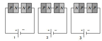
- A
In the circuit (1) and (2)
- ✓
In the circuit (2) and (3)
- C
In the circuit (1) and (3)
- D
AnswerCorrect option: B. In the circuit (2) and (3)
In the circuit (2) and (3)
View full question & answer→MCQ 2731 Mark
When a PN junction diode is reverse biased
- A
Electrons and holes are attracted towards each other and move towards the depletion region
- ✓
Electrons and holes move away from the junction depletion region
- C
Height of the potential barrier decreases
- D
No change in the current takes place
AnswerCorrect option: B. Electrons and holes move away from the junction depletion region
Electrons and holes move away from the junction depletion region
View full question & answer→MCQ 2741 Mark
The PN junction diode is used as
MCQ 2751 Mark
If the forward voltage in a semiconductor diode is doubled, the width of the depletion layer will
MCQ 2761 Mark
What is the current in the circuit shown below
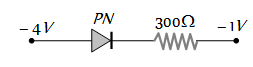
MCQ 2771 Mark
In the circuit given below, the value of the current is
- A
$0$ amp
- ✓
$10^{-2} amp$
- C
$10^2 amp$
- D
$10^{-3} amp$
AnswerCorrect option: B. $10^{-2} amp$
(b) $10^{-2} amp$
View full question & answer→MCQ 2781 Mark
The electrical resistance of depletion layer is large because
- ✓
It has no charge carriers
- B
It has a large number of charge carriers
- C
It contains electrons as charge carriers
- D
It has holes as charge carriers
AnswerCorrect option: A. It has no charge carriers
It has no charge carriers
View full question & answer→MCQ 2791 Mark
The reverse biasing in a PN junction diode
- A
Decreases the potential barrier
- ✓
Increases the potential barrier
- C
Increases the number of minority charge carriers
- D
Increases the number of majority charge carriers
AnswerCorrect option: B. Increases the potential barrier
Increases the potential barrier
View full question & answer→MCQ 2801 Mark
PN-junction diode works as a insulator, if connected
MCQ 2811 Mark
The electrical circuit used to get smooth dc output from a rectifier circuit is called
MCQ 2821 Mark
The cut-in voltage for silicon diode is approximately
MCQ 2831 Mark
In the forward bias arrangement of a PN-junction diode
- A
The N-end is connected to the positive terminal of the battery
- ✓
The P-end is connected to the positive terminal of the battery
- C
The direction of current is from N-end to P-end in the diode
- D
The P-end is connected to the negative terminal of battery
AnswerCorrect option: B. The P-end is connected to the positive terminal of the battery
The P-end is connected to the positive terminal of the battery
View full question & answer→MCQ 2841 Mark
In a junction diode, the holes are due to
MCQ 2851 Mark
The approximate ratio of resistances in the forward and reverse bias of the PN-junction diode is
- A
$10^2: 1$
- B
$10^{-2}: 1$
- C
$1: 10^{-4}$
- ✓
$1: 10^4$
AnswerCorrect option: D. $1: 10^4$
(d) $1: 10^4$
View full question & answer→MCQ 2861 Mark
A semiconductor device is connected in a series circuit with a battery and a resistance. A current is found to pass through the circuit. If the polarity of the battery is reversed, the current drops almost to zero. The device may be
- A
- B
- ✓
- D
An intrinsic semiconductor
View full question & answer→MCQ 2871 Mark
Which of the following statements concerning the depletion zone of an unbiased PN junction is (are) true
- A
The width of the zone is independent of the densities of the dopants (impurities)
- B
The width of the zone is dependent on the densities of the dopants
- C
The electric field in the zone is produced by the ionized dopant atoms
- ✓
View full question & answer→MCQ 2881 Mark
In the case of forward biasing of PN-junction, which one of the following figures correctly depicts the direction of flow of carriers
MCQ 2891 Mark
On increasing the reverse bias to a large value in a PN-junction diode, current
MCQ 2901 Mark
The energy gap of silicon is $1.14 eV. $The maximum wavelength at which silicon will begin absorbing energy is
- ✓
$10888 \mathring A$
- B
$1088.8 \mathring A$
- C
$108.88 \mathring A$
- D
$10.888 \mathring A$
AnswerCorrect option: A. $10888 \mathring A$
$10888 \mathring A$
View full question & answer→MCQ 2911 Mark
- ✓
The current in the reverse biased condition is generally very small
- B
The current in the reverse biased condition is small but the forward biased current is independent of the bias voltage
- C
The reverse biased current is strongly dependent on the applied bias voltage
- D
The forward biased current is very small in comparison to reverse biased current
AnswerCorrect option: A. The current in the reverse biased condition is generally very small
The current in the reverse biased condition is generally very small
View full question & answer→MCQ 2921 Mark
Doping of intrinsic semiconductor is done
- A
To neutralize charge carriers
- ✓
To increase the concentration of majority charge carriers
- C
To make it neutral before disposal
- D
To carry out further purification
AnswerCorrect option: B. To increase the concentration of majority charge carriers
To increase the concentration of majority charge carriers
View full question & answer→MCQ 2931 Mark
A semiconductor dopped with a donor impurity is
MCQ 2941 Mark
Carbon, silicon and Germanium atoms have four valence electrons each. Their valence and conduction band are separated by energy band gaps represented by $\left(E_g\right)_C \cdot\left(E_g\right)_{s i}$ and $\left(E_g\right)_{G e}$ respectively. Which one of the following relationship is true in their case
- ✓
$\left(E_g\right) C>\left(E_g\right) Si$
- B
$\left(E_g\right) C=\left(E_g\right) Si$
- C
$\left( E _{ g }\right) C <\left( E _{ g }\right) Ge$
- D
$\left( E _{ g }\right) C <\left( E _{ g }\right) Si$
AnswerCorrect option: A. $\left(E_g\right) C>\left(E_g\right) Si$
$\left(E_g\right) C>\left(E_g\right) Si$
View full question & answer→MCQ 2951 Mark
The energy band diagrams for three semiconductor samples of silicon are as shown. We can then assert that
- ✓
Sample X is undoped while samples Y and Z have been doped with a third group and a fifth group impurity respectively
- B
Sample X is undoped while both samples Y and Z have been doped with a fifth group impurity
- C
Sample X has been doped with equal amounts of third and fifth group impurities while samples Y and Z are undoped
- D
Sample X is undoped while samples Y and Z have been doped with a fifth group and a third group impurity respectively
AnswerCorrect option: A. Sample X is undoped while samples Y and Z have been doped with a third group and a fifth group impurity respectively
(a) Sample X is undoped while samples Y and Z have been doped with a third group and a fifth group impurity respectively
View full question & answer→MCQ 2961 Mark
Which of the energy band diagrams shown in the figure corresponds to that of a semiconductor
MCQ 2971 Mark
The electron mobility in $N-$type germanium is $3900 \mathrm{~cm}^2 / \mathrm{v}-s$ and its conductivity is $6.24 \ \mathrm{mho} / \mathrm{cm}$, then impurity concentration will be if the effect of cotters is negligible
- A
$ 10^{15} \mathrm{~cm}^3$
- B
$ 10^{13} / \mathrm{cm}^3$
- C
$ 10^{12} / \mathrm{cm}^3$
- ✓
$ 10^{16} / \mathrm{cm}^3$
AnswerCorrect option: D. $ 10^{16} / \mathrm{cm}^3$
$ 10^{16} / \mathrm{cm}^3$
View full question & answer→MCQ 2981 Mark
The relation between the number of free electrons in semiconductors (n) and its temperature (T) is
- A
$n \propto T^2$
- B
$n \propto T$
- C
$n \propto \sqrt{ T }$
- ✓
$n \propto T^{3 / 2}$
AnswerCorrect option: D. $n \propto T^{3 / 2}$
(d) $n \propto T^{3 / 2}$
View full question & answer→MCQ 2991 Mark
The mobility of free electron is greater than that of free holes because
- A
The carry negative charge
- B
- C
They mutually collide less
- ✓
They require low energy to continue their motion
AnswerCorrect option: D. They require low energy to continue their motion
They require low energy to continue their motion
View full question & answer→MCQ 3001 Mark
Which of the following energy band diagram shows the N-type semiconducto
MCQ 3011 Mark
To a germanium sample, traces of gallium are added as an impurity. The resultant sample would behave like
MCQ 3021 Mark
When phosphorus and antimony are mixed in zermaniun, then
- A
P-type semiconductor is formed
- ✓
N-type semiconductor is formed
- C
- D
AnswerCorrect option: B. N-type semiconductor is formed
N-type semiconductor is formed
View full question & answer→MCQ 3031 Mark
The process of adding impurities to the pure semiconductor is called
MCQ 3041 Mark
The energy band gap is maximum in
MCQ 3051 Mark
- A
There are no free electrons at any temperature
- B
The number of free electrons is more than that in a conductor
- ✓
There are no free electrons at 0 K
- D
AnswerCorrect option: C. There are no free electrons at 0 K
There are no free electrons at 0 K
View full question & answer→MCQ 3061 Mark
Which impurity is doped in Si to form N-type semi-conductor?
MCQ 3071 Mark
The valence band and conduction band of a solid overlap at low temperature, the solid may be
MCQ 3081 Mark
In intrinsic semiconductor at room temperature, number of electrons and holes are
MCQ 3091 Mark
Electric current is due to drift of electrons in
MCQ 3101 Mark
Resistivity of a semiconductor depends on
- A
- ✓
Atomic nature of semiconductor
- C
- D
Shape and atomic nature of semiconductor
AnswerCorrect option: B. Atomic nature of semiconductor
Atomic nature of semiconductor
View full question & answer→MCQ 3111 Mark
In extrinsic semiconductors
- A
The conduction band and valence band overlap
- B
The gap between conduction band and valence band is more than 16 eV
- ✓
The gap between conduction band and valence band is near about 1 eV
- D
The gap between conduction band and valence band will be 100 eV and more
AnswerCorrect option: C. The gap between conduction band and valence band is near about 1 eV
The gap between conduction band and valence band is near about 1 eV
View full question & answer→MCQ 3121 Mark
If $n_e$ and $v_d$ be the number of electrons and drift velocity in a semiconductor. When the temperature is increased
- ✓
$n_e$ increases and $v_d$ decreases
- B
$ {n}_ {e} $ decreases and $v_{\mathrm{d}}$ increases
- C
Both $\mathrm{n}_{\mathrm{e}}$ and $\mathrm{v}_{\mathrm{d}}$ increases
- D
Both $n_e$ and $v_d$ decreases
AnswerCorrect option: A. $n_e$ increases and $v_d$ decreases
$n_e$ increases and $v_d$ decreases
View full question & answer→MCQ 3131 Mark
Intrinsic semiconductor is electrically neutral. Extrinsic semiconductor having large number of current carriers would be
- A
- B
- C
Positively charged or negatively charged depending upon the type of impurity that has been added
- ✓
View full question & answer→MCQ 3141 Mark
A piece of semiconductor is connected in series in an electric circuit. On increasing the temperature, the current in the circuit will
MCQ 3151 Mark
In a P-type semi-conductor, germanium is dopped with
MCQ 3161 Mark
Choose the correct statement
- A
When we heat a semiconductor its resistance increases
- ✓
When we heat a semiconductor its resistance decreases
- C
When we cool a semiconductor to 0 K then it becomes super conductor
- D
Resistance of a semiconductor is independent of temperature
AnswerCorrect option: B. When we heat a semiconductor its resistance decreases
When we heat a semiconductor its resistance decrease
View full question & answer→MCQ 3171 Mark
Which of the following statements is true for an N-type semi-conductor
- ✓
The donor level lies closely below the bottom of the conduction band
- B
The donor level lies closely above the top of the valence band
- C
The donor level lies at the halfway mark of the forbidden energy gap
- D
AnswerCorrect option: A. The donor level lies closely below the bottom of the conduction band
The donor level lies closely below the bottom of the conduction band
View full question & answer→MCQ 3181 Mark
In semiconductors at a room temperature
- ✓
The valence band is partially empty and the conduction band is partially filled
- B
The valence band is completely filled and the conduction band is partially filled
- C
The valence band is completely filled
- D
The conduction band is completely empty
AnswerCorrect option: A. The valence band is partially empty and the conduction band is partially filled
The valence band is partially empty and the conduction band is partially filled
View full question & answer→MCQ 3191 Mark
Which of the following has negative temperature coefficient of resistance
MCQ 3201 Mark
When germanium is doped with phosphorus, the doped material has
- A
- B
- ✓
More negative current carriers
- D
More positive current carriers
AnswerCorrect option: C. More negative current carriers
More negative current carriers
View full question & answer→MCQ 3211 Mark
The charge on a hole is equal to the charge of
MCQ 3221 Mark
The difference in the variation of resistance with temperature in a metal and a semiconductor arises essentially due to the difference in the
- A
Variation of scattering mechanism with temperature
- B
- ✓
Variation of the number of charge carriers with temperature
- D
AnswerCorrect option: C. Variation of the number of charge carriers with temperature
Variation of the number of charge carriers with temperature
View full question & answer→MCQ 3231 Mark
Donor type impurity is found in
MCQ 3241 Mark
For non-conductors, the energy gap is
MCQ 3251 Mark
If $n _{ e }$ and $n _{ h }$ are the number of electrons and holes in a semiconductor heavily doped with phosphorus, then
- ✓
$n_e \gg n_h$
- B
$n_e \ll n_h$
- C
$n _{ e } \leq n _{ h }$
- D
$n _{ e }= n _{ h }$
AnswerCorrect option: A. $n_e \gg n_h$
$n_e \gg n_h$
View full question & answer→MCQ 3261 Mark
At room temperature, a P-type semiconductor has
- ✓
Large number of holes and few electrons
- B
Large number of free electrons and few holes
- C
Equal number of free electrons and holes
- D
AnswerCorrect option: A. Large number of holes and few electrons
Large number of holes and few electrons
View full question & answer→MCQ 3271 Mark
View full question & answer→MCQ 3281 Mark
Semiconductor is damaged by the strong current due to
MCQ 3291 Mark
In N-type semiconductors, majority charge carriers are
MCQ 3301 Mark
In a P-type semiconductor, germanium is doped with
MCQ 3311 Mark
When the temperature of silicon sample is increased from 27℃ to 100℃, the conductivity of silicon will be
MCQ 3321 Mark
At ordinary temperatures, the electrical conductivity of semi conductors in mho/meter is in the range
- A
$10^{-3}$ to $10^{-4}$
- ✓
$10^6$ to
- C
$10^{-6}$ to
- D
$10^{-10}$ to $10^{-16}$
AnswerCorrect option: B. $10^6$ to
$10^6$ to $10^9$
View full question & answer→MCQ 3331 Mark
P-type semiconductors are made by adding impurity element
MCQ 3341 Mark
The band gap in Germanium and silicon in eV respectively is
MCQ 3351 Mark
Which is the correct relation for forbidden energy gap in conductor, semi conductor and insulator
- A
$\Delta Eg _{ c }>\Delta Eg _{ sc }>\Delta Eg _{\text {insulator }}$
- ✓
$\Delta Eg _{\text {insulator }}>\Delta Eg _{ sc }>\Delta Eg _{\text {conductor }}$
- C
$\Delta Eg _{\text {conductor }}>\Delta Eg _{\text {insulator }}>\Delta Eg _{\text {sc }}$
- D
$\Delta Eg _{ sc }>\Delta Eg _{\text {conductor }}>\Delta Eg _{\text {insulator }}$
AnswerCorrect option: B. $\Delta Eg _{\text {insulator }}>\Delta Eg _{ sc }>\Delta Eg _{\text {conductor }}$
$\Delta Eg _{\text {insulator }}>\Delta Eg _{ sc }>\Delta Eg _{\text {conductor }}$
View full question & answer→MCQ 3361 Mark
A pure semiconductor behaves slightly as a conductor at
MCQ 3371 Mark
For germanium crystal, the forbidden energy gap in joules is
- ✓
$1.12 \times 10^{-19}$
- B
$1.76 \times 10^{-19}$
- C
$1.6 \times 10^{-19}$
- D
AnswerCorrect option: A. $1.12 \times 10^{-19}$
(a) $1.12 \times 10^{-19}$
View full question & answer→MCQ 3381 Mark
To obtain electrons as majority charge carriers in a semiconductor, the impurity mixed is
MCQ 3391 Mark
The state of the energy gained by valance electrons when the temperature is raised or when electric field is applied is called as
MCQ 3401 Mark
N-type semiconductors will be obtained, when germanium is doped with
MCQ 3411 Mark
An N-type and P-type silicon can be obtained by doping pure silicon with
MCQ 3421 Mark
Resistance of semiconductor at 0 K is
MCQ 3431 Mark
The addition of antimony atoms to a sample of intrinsic germanium transforms it to a material which is
MCQ 3441 Mark
The intrinsic semiconductor becomes an insulator at
MCQ 3451 Mark
In a semiconductor the separation between conduction band and valence band is of the order of
MCQ 3461 Mark
Fermi level of energy of an intrinsic semiconductor lies
- ✓
In the middle of forbidden gap
- B
Below the middle of forbidden gap
- C
Above the middle of forbidden gap
- D
Outside the forbidden gap
AnswerCorrect option: A. In the middle of forbidden gap
In the middle of forbidden gap
View full question & answer→MCQ 3471 Mark
(USS 133) Indium impurity in germanium makes
MCQ 3481 Mark
In intrinsic semiconductor at room temperature, number of electrons and holes are
MCQ 3491 Mark
If $N _{ p }$ and $N _{ e }$ be the numbers of holes and conduction electrons in an extrinsic semiconductor, then
AnswerCorrect option: D. $N _{ p }> N _{ e }$ or $N _{ p }< N _{ e }$ depending on the nature of impurity
(d) $N _{ p }> N _{ e }$ or $N _{ p }< N _{ e }$ depending on the nature of impurity
View full question & answer→MCQ 3501 Mark
A semiconductor is cooled from $T _1 K$ to $T _2 K$. Its resistance
- A
- ✓
- C
Will first decrease and then increase
- D
View full question & answer→MCQ 3511 Mark
In a P-type semiconductor
- ✓
Current is mainly carried by holes
- B
Current is mainly carried by electrons
- C
The material is always positively charged
- D
Doping is done by pentavalent material
AnswerCorrect option: A. Current is mainly carried by holes
Current is mainly carried by holes
View full question & answer→MCQ 3521 Mark
Energy bands in solids are a consequence of
- A
- ✓
Pauli’s exclusion principle
- C
- D
Heisenberg’s uncertainty principle
AnswerCorrect option: B. Pauli’s exclusion principle
Pauli’s exclusion principle
View full question & answer→MCQ 3531 Mark
In case of a semiconductor, which of the following statement is wrong
- A
Doping increases conductivity
- B
Temperature coefficient of resistance is negative
- C
Resisitivity is in between that of a conductor and insulator
- ✓
At absolute zero temperature, it behaves like a conductor
AnswerCorrect option: D. At absolute zero temperature, it behaves like a conductor
At absolute zero temperature, it behaves like a conductor
View full question & answer→MCQ 3541 Mark
$P-$ type semiconductor is formed when
$A$. As impurity is mixed in $Si$
$B. Al$ impurity is mixed in $Si$
$C. B$ impurity is mixed in $Ge$
$D. P$ impurity is mixed in $Ge$
- A
$A$ and $C$
- B
$A$ and $D$
- ✓
$B$ and $C$
- D
$B$ and $D$
AnswerCorrect option: C. $B$ and $C$
$B$ and $C$
View full question & answer→MCQ 3551 Mark
The temperature coefficient of resistance of a semiconductor
- A
- ✓
- C
- D
May be positive or negative or zero
View full question & answer→MCQ 3561 Mark
To obtain a P-type germanium semiconductor, it must be doped with
MCQ 3571 Mark
When N-type of semiconductor is heated
- A
Number of electrons increases while that of holes decreases
- B
Number of holes increases while that of electrons decreases
- C
Number of electrons and holes remains same
- ✓
Number of electrons and holes increases equally
AnswerCorrect option: D. Number of electrons and holes increases equally
Number of electrons and holes increases equally
View full question & answer→MCQ 3581 Mark
The impurity atom added to germanium to make it N-type semiconductor is
MCQ 3591 Mark
In a good conductor the energy gap between the conduction band and the valence band is
MCQ 3601 Mark
When a semiconductor is heated, its resistance
MCQ 3611 Mark
Electronic configuration of germanium is 2, 8, 18 and 4. To make it extrinsic semiconductor small quantity of antimony is added
- A
The material obtained will be N-type germanium in which electrons and holes are equal in number
- B
The material obtained will be P-type germanium
- ✓
The material obtained will be N-type germanium which has more electrons than holes at room temperature
- D
The material obtained will be N-type germanium which has less electrons than holes at room temperature
AnswerCorrect option: C. The material obtained will be N-type germanium which has more electrons than holes at room temperature
The material obtained will be N-type germanium which has more electrons than holes at room temperature
View full question & answer→MCQ 3621 Mark
At zero Kelvin a piece of germanium
MCQ 3631 Mark
In P-type semiconductor the majority and minority charge carriers are respectively
MCQ 3641 Mark
The forbidden gap in the energy bands of germanium at room temperature is about
MCQ 3651 Mark
A hole in a P-type semiconductor is
MCQ 3661 Mark
In extrinsic P and N-type, semiconductor materials, the ratio of the impurity atoms to the pure semiconductor atoms is about
- A
$1$
- B
$10^{-1}$
- C
$10^{-4}$
- ✓
$10^{-7}$
AnswerCorrect option: D. $10^{-7}$
$10^{-7}$
View full question & answer→MCQ 3671 Mark
Holes are charge carriers in
MCQ 3681 Mark
The impurity atoms which are mixed with pure silicon to make a P-type semiconductor are those of
MCQ 3691 Mark
Wires P and Q have the same resistance at ordinary (room) temperature. When heated, resistance of P increases and that of Q decreases. We conclude that
- A
P and Q are conductors of different materials
- B
P is N-type semiconductor and Q is P-type semiconductor
- C
P is semiconductor and Q is conductor
- ✓
P is conductor and Q is semiconductor
AnswerCorrect option: D. P is conductor and Q is semiconductor
P is conductor and Q is semiconductor
View full question & answer→MCQ 3701 Mark
Let $n _{ p }$ and $n _{ e }$ be the number of holes and conduction electrons respectively in a semiconductor. Then
- A
$n _{ p }> n _{ e }$ in an intrinsic semiconductor
- B
$n _{ p }= n _{ e }$ in an extrinsic semiconductor
- ✓
$n _{ p }= n _{ e }$ in an intrinsic semiconductor
- D
$n _{ e }> n _{ p }$ in an intrinsic semiconductor
AnswerCorrect option: C. $n _{ p }= n _{ e }$ in an intrinsic semiconductor
(c) $n _{ p }= n _{ e }$ in an intrinsic semiconductor
View full question & answer→MCQ 3711 Mark
When Ge crystals are doped with phosphorus atom, then it becomes
MCQ 3721 Mark
Which statement is correct
- A
N-type germanium is negatively charged and P-type germanium is positively charged
- ✓
Both N-type and P-type germanium are neutral
- C
N-type germanium is positively charged and P-type germanium is negatively charged
- D
Both N-type and P-type germanium are negatively charged
AnswerCorrect option: B. Both N-type and P-type germanium are neutral
Both N-type and P-type germanium are neutral
View full question & answer→MCQ 3731 Mark
The forbidden energy band gap in conductors, semiconductors and insulators are $EG _1, EG _2$ and $EG _3$ respectively. The relation among them is
- A
$EG _1= EG _2= EG _3$
- ✓
$EG _1< EG _2< EG _3$
- C
$EG _1> EG _2> EG _3$
- D
$EG _1< EG _2> EG _3$
AnswerCorrect option: B. $EG _1< EG _2< EG _3$
(b) $EG _1< EG _2< EG _3$
View full question & answer→MCQ 3741 Mark
The energy band gap of Si is
- A
- ✓
- C
Between 0.70 eV to 1.1 eV
- D
View full question & answer→MCQ 3751 Mark
In an insulator, the forbidden energy gap between the valence band and conduction band is of the order of
MCQ 3761 Mark
Three semi-conductors are arranged in the increasing order of their energy gap as follows. The correct arrangement is
- ✓
Tellurium, germanium, silicon
- B
Tellurium, silicon, germanium
- C
Silicon, germanium, tellurium
- D
Silicon, tellurium, germanium
AnswerCorrect option: A. Tellurium, germanium, silicon
Tellurium, germanium, silicon
View full question & answer→MCQ 3771 Mark
Electrical conductivity of a semiconductor
- A
Decreases with the rise in its temperature
- ✓
Increases with the rise in its temperature
- C
Does not change with the rise in its temperature
- D
First increases and then decreases with the rise in its temperature
AnswerCorrect option: B. Increases with the rise in its temperature
Increases with the rise in its temperature
View full question & answer→MCQ 3781 Mark
To obtain P-type Si semiconductor, we need to dope pure Si with
MCQ 3791 Mark
A piece of copper and the other of germanium are cooled from the room temperature to 80 K, then which of the following would be a correct statement
- A
Resistance of each increases
- B
Resistance of each decreases
- C
Resistance of copper increases while that of germanium decreases
- ✓
Resistance of copper decreases while that of germanium increases
AnswerCorrect option: D. Resistance of copper decreases while that of germanium increases
Resistance of copper decreases while that of germanium increases
View full question & answer→MCQ 3801 Mark
When the electrical conductivity of a semi- conductor is due to the breaking of its covalent bonds, then the semiconductor is said to be
MCQ 3811 Mark
Silicon is a semiconductor. If a small amount of As is added to it, then its electrical conductivity
MCQ 3821 Mark
The valence of the impurity atom that is to be added to germanium crystal so as to make it a N-type semiconductor, is
MCQ 3831 Mark
In P-type semiconductor, there is
- A
An excess of one electron
- ✓
- C
- D
View full question & answer→MCQ 3841 Mark
In a semiconductor, the concentration of electrons is $8 \times 10^{12} cm^3$ and that of the holes is $5 \times 10^{12} cm^3$. The semiconductor is
View full question & answer→MCQ 3851 Mark
The valence of an impurity added to germanium crystal in order to convert it into a P-type semi conductor is
MCQ 3861 Mark
A P-type semiconductor can be obtained by adding
- A
- ✓
- C
Antimony to pure germanium
- D
Phosphorous to pure germanium
View full question & answer→MCQ 3871 Mark
The majority charge carriers in P-type semiconductor are
MCQ 3881 Mark
Bonding in a germanium crystal (semi- conductor) is
MCQ 3891 Mark
A solid that transmits light in visible region and has a very low melting point possesses
MCQ 3901 Mark
The distance between the body centred atom and a corner atom in sodium (a = 4.225 Å) is
MCQ 3911 Mark
What is the coordination number of sodium ions in the case of sodium chloride structure
MCQ 3921 Mark
Crystal structure of NaCl is
MCQ 3931 Mark
In a crystal, the atoms are located at the position of
- A
- ✓
- C
- D
Infinite potential energy
View full question & answer→MCQ 3941 Mark
Which one of the following is the weakest kind of bonding in solids
MCQ 3951 Mark
Metallic solids are always opaque because
- A
Solids effect the incident light
- ✓
Incident light is readily absorbed by the free electron in a metal
- C
Incident light is scattered by solid molecules
- D
Energy band traps the incident light
AnswerCorrect option: B. Incident light is readily absorbed by the free electron in a metal
Incident light is readily absorbed by the free electron in a metal
View full question & answer→MCQ 3961 Mark
In a triclinic crystal system
MCQ 3971 Mark
Biaxial crystal among the following is
MCQ 3981 Mark
In good conductors of electricity, the type of bonding that exists is
MCQ 3991 Mark
Copper has face centered cubic (fcc) lattice with interatomic spacing equal to 2.54Å. The value of the lattice constant for this lattice is
MCQ 4001 Mark
Which of the following is an amorphous solid
MCQ 4011 Mark
Sodium has body centred packing. If the distance between two nearest atoms is 3.7 Å, then its lattice parameter is
MCQ 4021 Mark
What is the net force on a $\mathrm{Cl}^{-}$ placed at the centre of the bcc structure of CsCl
- ✓
- B
$ke ^2 / a ^2$
- C
$k^2 a^2$
- D
View full question & answer→MCQ 4031 Mark
The laptop PC’s modern electronic watches and calculators use the following for display
MCQ 4041 Mark
A solid reflects incident light and it’s electrical conductivity decreases with temperature. The binding in this solids
MCQ 4051 Mark
- A
$\frac{a}{2}$
- ✓
$\frac{a}{2 \sqrt{2}}$
- C
$\frac{\sqrt{3}}{4} a$
- D
$\frac{\sqrt{3}}{2} a$
AnswerCorrect option: B. $\frac{a}{2 \sqrt{2}}$
$\frac{a}{2 \sqrt{2}}$
View full question & answer→MCQ 4061 Mark
The coordination number of Cu is
MCQ 4071 Mark
Which of the following materials is non crystalline
MCQ 4081 Mark
In which of the following ionic bond is present
MCQ 4091 Mark
The expected energy of the electrons at absolute zero is called
MCQ 4101 Mark
The nature of binding for a crystal with alternate and evenly spaced positive and negative ions is
MCQ 4111 Mark
For a crystal system, $a = b = c, a = b = g^1\ 90^\circ$, the system is
View full question & answer→MCQ 4121 Mark
The temperature coefficient of resistance of a conductor is
MCQ 4131 Mark
Potassium has a $\ce{bcc}$ structure with nearest neighbour distance $4.525 \mathring A .$ Its molecular weight is $39.$ Its density in $kg/m^3$ is
View full question & answer→